DSP56309EVM Freescale Semiconductor, DSP56309EVM Datasheet - Page 248
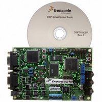
DSP56309EVM
Manufacturer Part Number
DSP56309EVM
Description
KIT EVALUATION FOR XC56309
Manufacturer
Freescale Semiconductor
Type
DSPr
Specifications of DSP56309EVM
Contents
Module Board, Installation Guide, Power Supply, Cable, Software and more
Description/function
Audio DSPs
Product
Audio Modules
For Use With/related Products
DSP56309
Lead Free Status / RoHS Status
Contains lead / RoHS non-compliant


Programming Reference
B-14
Application:
Bus Control Register (BCR)
Reset = $1FFFFF
BRH
NOTE: All BCR bits are read/write control bits.
23 22 21 20
Bus Request Hold, Bit 23
0 = BR pin is asserted only for attempted
1 = BR pin is always asserted
Bus Interface Unit
or pending access
*
0
BBS
Bus State, Bit 21
0 = DSP is not bus master
1 = DSP is bus master
19 18 17 16
BDFW[4–0]
Figure B-5. Bus Control Register (BCR)
15 14 13 12 11 10 9
DSP56309 User’s Manual, Rev. 1
BA3W[2–0]
X:$FFFFFB Read/Write
BA2W[2–0]
8
BA1W[4–0]
Default Area Wait Control, Bits 20–16
Area 3 Wait Control, Bits 15–13
Area 2 Wait Control, Bits 12–10
Area 0 Wait Control, Bits 4– 0
These read/write control bits define
the number of wait states inserted
into each external SRAM access to
the designated area. The value of
these bits should not be programmed
as zero.
Area 1 Wait Control, Bits 9–5
7
20–16
15–13
12–10
Bits
*
9–5
4–0
Date:
Programmer:
6
= Reserved, Program as 0
5
BDFW[4–0]
BA3W[2–0]
BA2W[2–0]
BA1W[4–0]
BA0W[4–0]
Bit Name
4
3
Freescale Semiconductor
BA0W[4–0]
# of Wait States
Sheet 1 of 2
2
0–31
0–31
0–31
0–7
0–7
1
0
Related parts for DSP56309EVM
Image
Part Number
Description
Manufacturer
Datasheet
Request
R

Part Number:
Description:
Manufacturer:
Freescale Semiconductor, Inc
Datasheet:
Part Number:
Description:
Manufacturer:
Freescale Semiconductor, Inc
Datasheet:
Part Number:
Description:
Manufacturer:
Freescale Semiconductor, Inc
Datasheet:
Part Number:
Description:
Manufacturer:
Freescale Semiconductor, Inc
Datasheet:
Part Number:
Description:
Manufacturer:
Freescale Semiconductor, Inc
Datasheet:
Part Number:
Description:
Manufacturer:
Freescale Semiconductor, Inc
Datasheet:
Part Number:
Description:
Manufacturer:
Freescale Semiconductor, Inc
Datasheet:
Part Number:
Description:
Manufacturer:
Freescale Semiconductor, Inc
Datasheet:
Part Number:
Description:
Manufacturer:
Freescale Semiconductor, Inc
Datasheet:
Part Number:
Description:
Manufacturer:
Freescale Semiconductor, Inc
Datasheet:
Part Number:
Description:
Manufacturer:
Freescale Semiconductor, Inc
Datasheet:
Part Number:
Description:
Manufacturer:
Freescale Semiconductor, Inc
Datasheet:
Part Number:
Description:
Manufacturer:
Freescale Semiconductor, Inc
Datasheet:
Part Number:
Description:
Manufacturer:
Freescale Semiconductor, Inc
Datasheet:
Part Number:
Description:
Manufacturer:
Freescale Semiconductor, Inc
Datasheet: