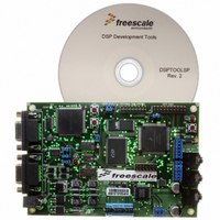
DSP56309EVM Freescale Semiconductor, DSP56309EVM Datasheet - Page 164
DSP56309EVM
Manufacturer Part Number
DSP56309EVM
Description
KIT EVALUATION FOR XC56309
Manufacturer
Freescale Semiconductor
Type
DSPr
Specifications of DSP56309EVM
Contents
Module Board, Installation Guide, Power Supply, Cable, Software and more
Description/function
Audio DSPs
Product
Audio Modules
For Use With/related Products
DSP56309
Lead Free Status / RoHS Status
Contains lead / RoHS non-compliant


Enhanced Synchronous Serial Interface (ESSI)
TSMA and TSMB (as in Figure 7-12 and Figure 7-13) can be seen as a single 32-bit register,
TSM. Bit n in TSM (TSn) is an enable/disable control bit for transmission in slot number N.
When TSn is cleared, all the data signals of the enabled transmitters are tri-stated during transmit
time slot number N. The data still transfers from the enabled transmit data register(s) to the
transmit shift register. However, the TDE and the TUE flags are not set. Consequently, during a
disabled slot, no transmitter empty interrupt is generated. The DSP is interrupted only for enabled
slots. Data written to the transmit data register when the transmitter empty interrupt request is
serviced transmits in the next enabled transmit time slot. When TSn is set, the transmit sequence
proceeds normally. Data transfers from the TX register to the shift register during slot number N,
and the TDE flag is set. The TSM slot mask does not conflict with the TSR. Even if a slot is
enabled in the TSM, you can chose to write to the TSR to tri-state the signals of the enabled
transmitters during the next transmission slot. Setting the bits in the TSM affects the next frame
transmission. The frame being transmitted is not affected by the new TSM setting. If the TSM is
read, it shows the current setting.
After a hardware
$FFFFFFFF, enabling all 32 slots for data transmission.
7.5.10 Receive Slot Mask Registers (RSMA, RSMB)
Both receive slot mask registers are read/write registers. In Network mode, the receiver(s) use
these registers to determine which action to take in the current time slot. Depending on the setting
of the bits, the receiver(s) either tri-state the receiver(s) data signal(s) or receive a data word and
generate a receiver full condition.
7-32
TS27
RS11
23
11
23
11
—Reserved bit; read as 0; write to 0 0 for future compatibility.
—Reserved bit; read as 0; write to 0 0 for future compatibility.
TS26
RS10
22
10
22
10
RESET
TS25
Figure 7-15. ESSI Transmit Slot Mask Register B (TSMB)
RS9
Figure 7-16. ESSI Receive Slot Mask Register A (RSMA)
21
21
9
9
signal or software RESET instruction, the TSM register is reset to
TS24
RS8
20
20
8
8
(ESSI0 X:$FFFFB3, ESSI1 X:$FFFFA3)
(ESSI0 X:$FFFFB2, ESSI1 X:$FFFFA2)
TS23
RS7
DSP56309 User’s Manual, Rev. 1
19
19
7
7
TS22
RS6
18
18
6
6
TS21
RS5
17
17
5
5
TS20
RS4
16
16
4
4
RS15
TS31
TS19
RS3
15
15
3
3
RS14
TS30
TS18
RS2
14
14
2
2
Freescale Semiconductor
RS13
TS29
TS17
RS1
13
13
1
1
RS12
TS28
TS16
RS0
12
12
0
0
Related parts for DSP56309EVM
Image
Part Number
Description
Manufacturer
Datasheet
Request
R

Part Number:
Description:
Manufacturer:
Freescale Semiconductor, Inc
Datasheet:
Part Number:
Description:
Manufacturer:
Freescale Semiconductor, Inc
Datasheet:
Part Number:
Description:
Manufacturer:
Freescale Semiconductor, Inc
Datasheet:
Part Number:
Description:
Manufacturer:
Freescale Semiconductor, Inc
Datasheet:
Part Number:
Description:
Manufacturer:
Freescale Semiconductor, Inc
Datasheet:
Part Number:
Description:
Manufacturer:
Freescale Semiconductor, Inc
Datasheet:
Part Number:
Description:
Manufacturer:
Freescale Semiconductor, Inc
Datasheet:
Part Number:
Description:
Manufacturer:
Freescale Semiconductor, Inc
Datasheet:
Part Number:
Description:
Manufacturer:
Freescale Semiconductor, Inc
Datasheet:
Part Number:
Description:
Manufacturer:
Freescale Semiconductor, Inc
Datasheet:
Part Number:
Description:
Manufacturer:
Freescale Semiconductor, Inc
Datasheet:
Part Number:
Description:
Manufacturer:
Freescale Semiconductor, Inc
Datasheet:
Part Number:
Description:
Manufacturer:
Freescale Semiconductor, Inc
Datasheet:
Part Number:
Description:
Manufacturer:
Freescale Semiconductor, Inc
Datasheet:
Part Number:
Description:
Manufacturer:
Freescale Semiconductor, Inc
Datasheet: