DSP56309EVM Freescale Semiconductor, DSP56309EVM Datasheet - Page 194
DSP56309EVM
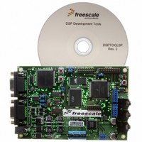
Manufacturer Part Number
DSP56309EVM
Description
KIT EVALUATION FOR XC56309
Manufacturer
Freescale Semiconductor
Type
DSPr
Specifications of DSP56309EVM
Contents
Module Board, Installation Guide, Power Supply, Cable, Software and more
Description/function
Audio DSPs
Product
Audio Modules
For Use With/related Products
DSP56309
Lead Free Status / RoHS Status
Contains lead / RoHS non-compliant


Triple Timer Module
9.1.2 Individual Timer Block Diagram
Figure 9-2 shows the structure of an individual timer block. The DSP56309 treats each timer as a
memory-mapped peripheral with four registers occupying four 24-bit words in the X data
memory space. The three timers are identical in structure and function. Either standard polled or
interrupt programming techniques can be used to service the timers. A single, generic timer is
discussed in this chapter. Each timer includes the following:
The timer mode is controlled by the TC[3–0] bits which are TCSR[7–4]. For a listing of the timer
modes and descriptions of their operations, see Section 9.3, Operating Modes, on page 9-5.
9-2
24-bit counter
24-bit read/write Timer Control and Status Register (TCSR)
24-bit read-only Timer Count Register (TCR)
24-bit write-only Timer Load Register (TLR)
24-bit read/write Timer Compare Register (TCPR)
Logic for clock selection and interrupt/DMA trigger generation.
GDB
Timer Prescaler
Load Register
24
CLK/2
TPLR
24-bit Counter
Figure 9-1. Triple Timer Module Block Diagram
TIO0 TIO1 TIO2
Timer Prescaler
Count Register
24
DSP56309 User’s Manual, Rev. 1
TPCR
24
Timer 0
Timer 1
Timer 2
24
Freescale Semiconductor
Related parts for DSP56309EVM
Image
Part Number
Description
Manufacturer
Datasheet
Request
R

Part Number:
Description:
Manufacturer:
Freescale Semiconductor, Inc
Datasheet:
Part Number:
Description:
Manufacturer:
Freescale Semiconductor, Inc
Datasheet:
Part Number:
Description:
Manufacturer:
Freescale Semiconductor, Inc
Datasheet:
Part Number:
Description:
Manufacturer:
Freescale Semiconductor, Inc
Datasheet:
Part Number:
Description:
Manufacturer:
Freescale Semiconductor, Inc
Datasheet:
Part Number:
Description:
Manufacturer:
Freescale Semiconductor, Inc
Datasheet:
Part Number:
Description:
Manufacturer:
Freescale Semiconductor, Inc
Datasheet:
Part Number:
Description:
Manufacturer:
Freescale Semiconductor, Inc
Datasheet:
Part Number:
Description:
Manufacturer:
Freescale Semiconductor, Inc
Datasheet:
Part Number:
Description:
Manufacturer:
Freescale Semiconductor, Inc
Datasheet:
Part Number:
Description:
Manufacturer:
Freescale Semiconductor, Inc
Datasheet:
Part Number:
Description:
Manufacturer:
Freescale Semiconductor, Inc
Datasheet:
Part Number:
Description:
Manufacturer:
Freescale Semiconductor, Inc
Datasheet:
Part Number:
Description:
Manufacturer:
Freescale Semiconductor, Inc
Datasheet:
Part Number:
Description:
Manufacturer:
Freescale Semiconductor, Inc
Datasheet: