DSP56309EVM Freescale Semiconductor, DSP56309EVM Datasheet - Page 42
DSP56309EVM
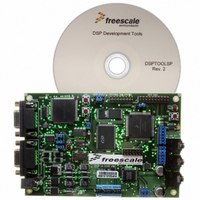
Manufacturer Part Number
DSP56309EVM
Description
KIT EVALUATION FOR XC56309
Manufacturer
Freescale Semiconductor
Type
DSPr
Specifications of DSP56309EVM
Contents
Module Board, Installation Guide, Power Supply, Cable, Software and more
Description/function
Audio DSPs
Product
Audio Modules
For Use With/related Products
DSP56309
Lead Free Status / RoHS Status
Contains lead / RoHS non-compliant


Signals/Connections
2.10 Serial Communication Interface (SCI)
The Serial Communication interface (SCI) provides a full duplex port for serial communication
with other DSPs, microprocessors, or peripherals such as modems.
2-18
RXD
PE0
TXD
PE1
SCLK
PE2
Notes: 1.
Signal
Name
2.
Input
Input or Output
Output
Input or Output
Input/Output
Input or Output
In the Stop state, the signal maintains the last state as follows:
•
•
The Wait processing state does not affect the signal state.
If the last state is input, the signal is an ignored input.
If the last state is output, these lines are tri-stated.
Type
Table 2-14. Serial Communication Interface (SCI)
Ignored input
Ignored input
Ignored input
State During
Reset
1, 2
DSP56309 User’s Manual, Rev. 1
Serial Receive Data
Receives byte-oriented serial data and transfers it to the SCI receive
shift register.
Port E 0
The default configuration following reset is GPIO. When configured as
PE0, signal direction is controlled through the Port E Directions Register
(PRRE). This signal is configured as RXD or PE0 through the Port E
Control Register (PCRE). This input is 5 V tolerant.
Serial Transmit Data
Transmits data from SCI transmit data register.
Port E 1
The default configuration following reset is GPIO. When configured as
PE1, signal direction is controlled through the SCI PRRE. This signal is
configured as TXD or PE1 through PCRE. This input is 5 V tolerant.
Serial Clock
Provides the input or output clock used by the transmitter and/or the
receiver.
Port E 2
The default configuration following reset is GPIO. For PE2, signal
direction is controlled through the SCI PRRE. This signal is configured
as SCLK or PE2 through PCRE. This input is 5 V tolerant.
Signal Description
Freescale Semiconductor
Related parts for DSP56309EVM
Image
Part Number
Description
Manufacturer
Datasheet
Request
R

Part Number:
Description:
Manufacturer:
Freescale Semiconductor, Inc
Datasheet:
Part Number:
Description:
Manufacturer:
Freescale Semiconductor, Inc
Datasheet:
Part Number:
Description:
Manufacturer:
Freescale Semiconductor, Inc
Datasheet:
Part Number:
Description:
Manufacturer:
Freescale Semiconductor, Inc
Datasheet:
Part Number:
Description:
Manufacturer:
Freescale Semiconductor, Inc
Datasheet:
Part Number:
Description:
Manufacturer:
Freescale Semiconductor, Inc
Datasheet:
Part Number:
Description:
Manufacturer:
Freescale Semiconductor, Inc
Datasheet:
Part Number:
Description:
Manufacturer:
Freescale Semiconductor, Inc
Datasheet:
Part Number:
Description:
Manufacturer:
Freescale Semiconductor, Inc
Datasheet:
Part Number:
Description:
Manufacturer:
Freescale Semiconductor, Inc
Datasheet:
Part Number:
Description:
Manufacturer:
Freescale Semiconductor, Inc
Datasheet:
Part Number:
Description:
Manufacturer:
Freescale Semiconductor, Inc
Datasheet:
Part Number:
Description:
Manufacturer:
Freescale Semiconductor, Inc
Datasheet:
Part Number:
Description:
Manufacturer:
Freescale Semiconductor, Inc
Datasheet:
Part Number:
Description:
Manufacturer:
Freescale Semiconductor, Inc
Datasheet: