DSP56309EVM Freescale Semiconductor, DSP56309EVM Datasheet - Page 14
DSP56309EVM
Manufacturer Part Number
DSP56309EVM
Description
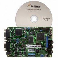
KIT EVALUATION FOR XC56309
Manufacturer
Freescale Semiconductor
Type
DSPr
Specifications of DSP56309EVM
Contents
Module Board, Installation Guide, Power Supply, Cable, Software and more
Description/function
Audio DSPs
Product
Audio Modules
For Use With/related Products
DSP56309
Lead Free Status / RoHS Status
Contains lead / RoHS non-compliant


DSP56309 Overview
1.4 Features
The Freescale DSP56309, a member of the DSP56300 core family of programmable DSPs,
supports wireless infrastructure applications with general filtering operations. Like the other
family members, the DSP56309 uses a high-performance, single-clock-cycle- per-instruction
engine (code compatible with Freescale's popular DSP56000 core family), a barrel shifter, 24-bit
addressing, instruction cache, and DMA controller. The DSP56309 offers 100 million
instructions per second (MIPS) performance using an internal 100 MHz clock with 3.3 V core
and input/output (I/O) power.
All DSP56300 core family members contain the DSP56300 core and additional modules. The
modules are chosen from a library of standard predesigned elements, such as memories and
peripherals. New modules can be added to the library to meet customer specifications. A standard
interface between the DSP56300 core and the internal memory and peripherals supports a wide
variety of memory and peripheral configurations. In particular, the DSP56309 includes a JTAG
port integrated with the Freescale OnCE module.
The DSP56309 is intended for use in telecommunication applications, such as multi-line
voice/data/fax processing, video conferencing, audio applications, control, and general digital
signal processing
1.5 DSP56300 Core
Core features are fully described in the DSP56300 Family Manual. This manual, in contrast,
documents pinout, memory, and peripheral features. Core features are as follows:
1-4
Modified signal definitions. In Table 2-11, changed the title of the third column to State
During Reset
the State During Reset of all signals to “Ignored input.” Changed the signal
description for PB14.
Modified signal definitions. In Table 2-12 to Table 2-15, deleted the Stop column.
Changed the title of the third column to State During Reset
changed the old note 1 to note 2.
Operating Mode Register layout and definition. Replaced Figure 4-2.
In Section 8.6.4.1, changed the beginning of the fourth paragraph from “In
Synchronous mode” to “In Asynchronous mode.”
Updated programming sheets. Replaced the programming sheets for the following
registers:
• Figure B-2, Operating Mode Register (OMR) (old Figure D-2)
• Figure B-21, Timer Load, Compare, and Count Registers (TLR, TCPR, and TCR)
(old Figure D-21)
1,2
Added a new note 1 and changed the old note 1 to note 2. Changed
Table 1-2. Change History, Revision 0 to Revision 1 (Continued)
Change
DSP56309 User’s Manual, Rev. 1
1,2
Added a new note 1 and
Pages 2-17 to
2-21
Page 2-22 to
2-31
Page 4-17
Page 8-20
Page D-13
Page D-33
Page Number
Revision 0
Freescale Semiconductor
Page 4-13
Page 8-21
Pages 2-10 to
2-12
Page 2-13 to
2-19
Page B-11
Page B-30
Page Number
Revision 1
Related parts for DSP56309EVM
Image
Part Number
Description
Manufacturer
Datasheet
Request
R

Part Number:
Description:
Manufacturer:
Freescale Semiconductor, Inc
Datasheet:
Part Number:
Description:
Manufacturer:
Freescale Semiconductor, Inc
Datasheet:
Part Number:
Description:
Manufacturer:
Freescale Semiconductor, Inc
Datasheet:
Part Number:
Description:
Manufacturer:
Freescale Semiconductor, Inc
Datasheet:
Part Number:
Description:
Manufacturer:
Freescale Semiconductor, Inc
Datasheet:
Part Number:
Description:
Manufacturer:
Freescale Semiconductor, Inc
Datasheet:
Part Number:
Description:
Manufacturer:
Freescale Semiconductor, Inc
Datasheet:
Part Number:
Description:
Manufacturer:
Freescale Semiconductor, Inc
Datasheet:
Part Number:
Description:
Manufacturer:
Freescale Semiconductor, Inc
Datasheet:
Part Number:
Description:
Manufacturer:
Freescale Semiconductor, Inc
Datasheet:
Part Number:
Description:
Manufacturer:
Freescale Semiconductor, Inc
Datasheet:
Part Number:
Description:
Manufacturer:
Freescale Semiconductor, Inc
Datasheet:
Part Number:
Description:
Manufacturer:
Freescale Semiconductor, Inc
Datasheet:
Part Number:
Description:
Manufacturer:
Freescale Semiconductor, Inc
Datasheet:
Part Number:
Description:
Manufacturer:
Freescale Semiconductor, Inc
Datasheet: