DSP56309EVM Freescale Semiconductor, DSP56309EVM Datasheet - Page 245
DSP56309EVM
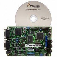
Manufacturer Part Number
DSP56309EVM
Description
KIT EVALUATION FOR XC56309
Manufacturer
Freescale Semiconductor
Type
DSPr
Specifications of DSP56309EVM
Contents
Module Board, Installation Guide, Power Supply, Cable, Software and more
Description/function
Audio DSPs
Product
Audio Modules
For Use With/related Products
DSP56309
Lead Free Status / RoHS Status
Contains lead / RoHS non-compliant


Freescale Semiconductor
Application:
23
*
0
Operating Mode Register
Reset = $00030X; X = latched from levels on Mode pins
Address Trace Enable, Bit 15
0 = Address Trace mode disabled
1 = Address Trace mode enabled
Stack Extension X Y Select, Bit 16
0 = Mapped to X memory
1 = Mapped to Y memory
Stack Extension Underflow Flag, Bit 17
0 = No stack underflow
1 = Stack underflow
Stack Extension Enable, Bit 20
0 = Stack extension disabled
1 = Stack extension enabled
Stack Extension Overflow Flag, Bit 18
0 = No stack overflow
1 = Stack overflow
Stack Extension Wrap Flag, Bit 19
0 = No stack extension wrap
1 = Stack extension wrap (sticky bit)
Asynchronous Bus Arbitration Enable, Bit 13
Central Processor
Address Attribute Priority Disable, Bit 14
0 = Synchronization disabled
1 = Synchronization enabled
0 = Priority mechanism enabled
1 = Priority mechanism disabled
22
*
0
21 20
*
0
SEN
WRP EOV
19 18 17 16
Figure B-2. Operating Mode Register (OMR)
EUN
XYS
DSP56309 User’s Manual, Rev. 1
15 14 13 12 11 10 9
ATE
APD ABE
Bus Release Timing, Bit 12
0 = Fast Bus Release mode
1 = Slow Bus Release mode
BRT TAS
Cache Burst Mode Enable, Bit 10
0 = Burst Mode disabled
1 = Burst Mode enabled
BE
TA Synchronize Select, Bit 11
0 = Not synchronized
1 = Synchronized
CPD1
CPD[1:0]
Core-DMA Priority, Bits 9–8
00
01
10
11
CPD0
1 = Memory switching enabled
Memory Switch Mode, Bit 7
0 = Memory switching disabled
8
Stop Delay Mode, Bit 6
0 = Delay is 128K clock cycles
1 = Delay is 16 clock cycles
MS
7
Compare SR[CP] to
active DMA channel
priority
DMA has higher
priority than core
DMA has same
priority as core
DMA has lower
priority than core
*
Date:
Programmer:
External Bus Disable, Bit 4
0 = Enables external bus
1 = Disables external bus
Chip Operating Mode, Bits 3–0
Refer to the operating modes
table in Chapter 4.
SD
6
= Reserved, Program as 0
Description
*
0
5
EBD
4
MD
3
Programming Sheets
Sheet 2 of 2
MC MB
2
1
MA
0
B-11
Related parts for DSP56309EVM
Image
Part Number
Description
Manufacturer
Datasheet
Request
R

Part Number:
Description:
Manufacturer:
Freescale Semiconductor, Inc
Datasheet:
Part Number:
Description:
Manufacturer:
Freescale Semiconductor, Inc
Datasheet:
Part Number:
Description:
Manufacturer:
Freescale Semiconductor, Inc
Datasheet:
Part Number:
Description:
Manufacturer:
Freescale Semiconductor, Inc
Datasheet:
Part Number:
Description:
Manufacturer:
Freescale Semiconductor, Inc
Datasheet:
Part Number:
Description:
Manufacturer:
Freescale Semiconductor, Inc
Datasheet:
Part Number:
Description:
Manufacturer:
Freescale Semiconductor, Inc
Datasheet:
Part Number:
Description:
Manufacturer:
Freescale Semiconductor, Inc
Datasheet:
Part Number:
Description:
Manufacturer:
Freescale Semiconductor, Inc
Datasheet:
Part Number:
Description:
Manufacturer:
Freescale Semiconductor, Inc
Datasheet:
Part Number:
Description:
Manufacturer:
Freescale Semiconductor, Inc
Datasheet:
Part Number:
Description:
Manufacturer:
Freescale Semiconductor, Inc
Datasheet:
Part Number:
Description:
Manufacturer:
Freescale Semiconductor, Inc
Datasheet:
Part Number:
Description:
Manufacturer:
Freescale Semiconductor, Inc
Datasheet:
Part Number:
Description:
Manufacturer:
Freescale Semiconductor, Inc
Datasheet: