DSP56309EVM Freescale Semiconductor, DSP56309EVM Datasheet - Page 187
DSP56309EVM
Manufacturer Part Number
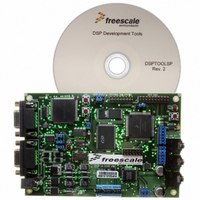
DSP56309EVM
Description
KIT EVALUATION FOR XC56309
Manufacturer
Freescale Semiconductor
Type
DSPr
Specifications of DSP56309EVM
Contents
Module Board, Installation Guide, Power Supply, Cable, Software and more
Description/function
Audio DSPs
Product
Audio Modules
For Use With/related Products
DSP56309
Lead Free Status / RoHS Status
Contains lead / RoHS non-compliant


and the external clock is used if the SCI is the slave device, as noted above. The clock is gated
and limited to a maximum frequency equal to one eighth of the DSP core operating frequency
(that is, 12.5 MHz for a DSP core frequency of 100 MHz).
For asynchronous operation, the SCI can use the internal and external clocks in any combination
as the source clocks for the TX clock and RX clock. If an external clock is used for the
input, it must be sixteen times the desired bit rate (designated as the 16
Figure 8-6. When the internal clock is used to supply a clock to an external device, the clock can
use the actual bit rate (designated as the 1
COD bit. The output clock is continuous.
When SCKP is cleared, the transmitted data on the
the serial clock and is stable on the positive edge. When SCKP is set, the data changes on the
positive edge and is stable on the negative edge. The received data on the
on the positive edge (if SCKP = 0) or on the negative edge (if SCKP = 1) of the serial clock.
8.6.4 SCI Data Registers
The SCI data registers are divided into two groups: receive and transmit, as shown in Figure 8-7.
There are two receive registers: a Receive Data Register (SRX) and a serial-to-parallel Receive
Shift Register. There are also two transmit registers: a Transmit Data Register (called either STX
or STXA) and a parallel-to-serial Transmit Shift Register.
Freescale Semiconductor
RX, TX Data
(SSFTD = 0)
(SCKP = 0)
x16 Clock
x1 Clock
Idle Line
Start
Figure 8-6. 16 x Serial Clock
DSP56309 User’s Manual, Rev. 1
0
1
×
clock) or the 16
2
3
TXD
4
signal changes on the negative edge of
5
×
Select 8-or 9-bit Words
6
clock rate, as determined by the
7
×
8
clock), as indicated in
RXD
Stop
SCI Programming Model
signal is sampled
Start
SCLK
8-19
Related parts for DSP56309EVM
Image
Part Number
Description
Manufacturer
Datasheet
Request
R

Part Number:
Description:
Manufacturer:
Freescale Semiconductor, Inc
Datasheet:
Part Number:
Description:
Manufacturer:
Freescale Semiconductor, Inc
Datasheet:
Part Number:
Description:
Manufacturer:
Freescale Semiconductor, Inc
Datasheet:
Part Number:
Description:
Manufacturer:
Freescale Semiconductor, Inc
Datasheet:
Part Number:
Description:
Manufacturer:
Freescale Semiconductor, Inc
Datasheet:
Part Number:
Description:
Manufacturer:
Freescale Semiconductor, Inc
Datasheet:
Part Number:
Description:
Manufacturer:
Freescale Semiconductor, Inc
Datasheet:
Part Number:
Description:
Manufacturer:
Freescale Semiconductor, Inc
Datasheet:
Part Number:
Description:
Manufacturer:
Freescale Semiconductor, Inc
Datasheet:
Part Number:
Description:
Manufacturer:
Freescale Semiconductor, Inc
Datasheet:
Part Number:
Description:
Manufacturer:
Freescale Semiconductor, Inc
Datasheet:
Part Number:
Description:
Manufacturer:
Freescale Semiconductor, Inc
Datasheet:
Part Number:
Description:
Manufacturer:
Freescale Semiconductor, Inc
Datasheet:
Part Number:
Description:
Manufacturer:
Freescale Semiconductor, Inc
Datasheet:
Part Number:
Description:
Manufacturer:
Freescale Semiconductor, Inc
Datasheet: