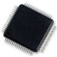
S9S12HY64J0MLH Freescale Semiconductor, S9S12HY64J0MLH Datasheet - Page 104

S9S12HY64J0MLH
Manufacturer Part Number
S9S12HY64J0MLH
Description
MCU 64K FLASH AUTO 64-LQFP
Manufacturer
Freescale Semiconductor
Series
HCS12r
Datasheet
1.S9S12HA32J0CLL.pdf
(792 pages)
Specifications of S9S12HY64J0MLH
Core Processor
HCS12
Core Size
16-Bit
Speed
32MHz
Connectivity
CAN, EBI/EMI, I²C, IrDA, LIN, SCI, SPI
Peripherals
LCD, Motor control PWM, POR, PWM, WDT
Number Of I /o
50
Program Memory Size
64KB (64K x 8)
Program Memory Type
FLASH
Eeprom Size
4K x 8
Ram Size
4K x 8
Voltage - Supply (vcc/vdd)
4.5 V ~ 5.5 V
Data Converters
A/D 6x10b
Oscillator Type
Internal
Operating Temperature
-40°C ~ 125°C
Package / Case
64-LQFP
Controller Family/series
S12
No. Of I/o's
50
Ram Memory Size
4KB
Cpu Speed
64MHz
No. Of Timers
2
Rohs Compliant
Yes
Processor Series
S12HY
Core
HCS12
3rd Party Development Tools
EWHCS12
Development Tools By Supplier
DEMO9S12HY64
Lead Free Status / RoHS Status
Lead free / RoHS Compliant
Available stocks
Company
Part Number
Manufacturer
Quantity
Price
Company:
Part Number:
S9S12HY64J0MLH
Manufacturer:
Freescale Semiconductor
Quantity:
10 000
- Current page: 104 of 792
- Download datasheet (4Mb)
1
1
Port Integration Module (S12HYPIMV1)
2.3.51
2.3.52
104
Address 0x0273
DDR1AD
Address 0x0274
Read: Anytime
Write: Anytime
Read: Always reads 0x00
Write: Unimplemented
Field
Reset
Reset
7-0
W
W
R
R
DDR1AD7
Port AD data direction—
This bit determines whether the associated pin is an input or output.
To use the digital input function the ATD Digital Input Enable Register (ATDDIEN) has to be set to logic level “1”.
1 Associated pin is configured as output
0 Associated pin is configured as input
Port AD Data Direction Register (DDR1AD)
PIM Reserved Register
0
0
0
7
7
Due to internal synchronization circuits, it can take up to 2 bus clock cycles
until the correct value is read on PT1AD registers, when changing the
DDR1AD register.
= Unimplemented or Reserved
DDR1AD6
Figure 2-49. Port AD Data Direction Register (DDR1AD)
0
0
0
6
6
Table 2-44. DDR1AD Register Field Descriptions
MC9S12HY/HA-Family Reference Manual, Rev. 1.04
DDR1AD5
Figure 2-50. PIM Reserved Register
0
0
0
5
5
DDR1AD4
NOTE
0
0
0
4
4
Description
DDR1AD3
3
0
3
0
0
DDR1AD2
0
0
0
2
2
DDR1AD1
Freescale Semiconductor
Access: User read/write
0
0
0
1
1
Access: User read
DDR1AD0
0
0
0
0
0
1
1
Related parts for S9S12HY64J0MLH
Image
Part Number
Description
Manufacturer
Datasheet
Request
R
Part Number:
Description:
Manufacturer:
Freescale Semiconductor, Inc
Datasheet:
Part Number:
Description:
Manufacturer:
Freescale Semiconductor, Inc
Datasheet:
Part Number:
Description:
Manufacturer:
Freescale Semiconductor, Inc
Datasheet:
Part Number:
Description:
Manufacturer:
Freescale Semiconductor, Inc
Datasheet:
Part Number:
Description:
Manufacturer:
Freescale Semiconductor, Inc
Datasheet:
Part Number:
Description:
Manufacturer:
Freescale Semiconductor, Inc
Datasheet:
Part Number:
Description:
Manufacturer:
Freescale Semiconductor, Inc
Datasheet:
Part Number:
Description:
Manufacturer:
Freescale Semiconductor, Inc
Datasheet:
Part Number:
Description:
Manufacturer:
Freescale Semiconductor, Inc
Datasheet:
Part Number:
Description:
Manufacturer:
Freescale Semiconductor, Inc
Datasheet:
Part Number:
Description:
Manufacturer:
Freescale Semiconductor, Inc
Datasheet:
Part Number:
Description:
Manufacturer:
Freescale Semiconductor, Inc
Datasheet:
Part Number:
Description:
Manufacturer:
Freescale Semiconductor, Inc
Datasheet:
Part Number:
Description:
Manufacturer:
Freescale Semiconductor, Inc
Datasheet:
Part Number:
Description:
Manufacturer:
Freescale Semiconductor, Inc
Datasheet:


