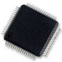
S9S12HY64J0MLH Freescale Semiconductor, S9S12HY64J0MLH Datasheet - Page 416

S9S12HY64J0MLH
Manufacturer Part Number
S9S12HY64J0MLH
Description
MCU 64K FLASH AUTO 64-LQFP
Manufacturer
Freescale Semiconductor
Series
HCS12r
Datasheet
1.S9S12HA32J0CLL.pdf
(792 pages)
Specifications of S9S12HY64J0MLH
Core Processor
HCS12
Core Size
16-Bit
Speed
32MHz
Connectivity
CAN, EBI/EMI, I²C, IrDA, LIN, SCI, SPI
Peripherals
LCD, Motor control PWM, POR, PWM, WDT
Number Of I /o
50
Program Memory Size
64KB (64K x 8)
Program Memory Type
FLASH
Eeprom Size
4K x 8
Ram Size
4K x 8
Voltage - Supply (vcc/vdd)
4.5 V ~ 5.5 V
Data Converters
A/D 6x10b
Oscillator Type
Internal
Operating Temperature
-40°C ~ 125°C
Package / Case
64-LQFP
Controller Family/series
S12
No. Of I/o's
50
Ram Memory Size
4KB
Cpu Speed
64MHz
No. Of Timers
2
Rohs Compliant
Yes
Processor Series
S12HY
Core
HCS12
3rd Party Development Tools
EWHCS12
Development Tools By Supplier
DEMO9S12HY64
Lead Free Status / RoHS Status
Lead free / RoHS Compliant
Available stocks
Company
Part Number
Manufacturer
Quantity
Price
Company:
Part Number:
S9S12HY64J0MLH
Manufacturer:
Freescale Semiconductor
Quantity:
10 000
- Current page: 416 of 792
- Download datasheet (4Mb)
Pulse-Width Modulator (S12PWM8B8CV1)
As an example of a center aligned output, consider the following case:
Shown in
11.4.2.7
The PWM timer also has the option of generating 8-channels of 8-bits or 4-channels of 16-bits for greater
PWM resolution. This 16-bit channel option is achieved through the concatenation of two 8-bit channels.
The PWMCTL register contains four control bits, each of which is used to concatenate a pair of PWM
channels into one 16-bit channel. Channels 6 and 7 are concatenated with the CON67 bit, channels 4 and
5 are concatenated with the CON45 bit, channels 2 and 3 are concatenated with the CON23 bit, and
channels 0 and 1 are concatenated with the CON01 bit.
When channels 6 and 7 are concatenated, channel 6 registers become the high order bytes of the double
byte channel, as shown in
registers become the high order bytes of the double byte channel. When channels 2 and 3 are concatenated,
channel 2 registers become the high order bytes of the double byte channel. When channels 0 and 1 are
concatenated, channel 0 registers become the high order bytes of the double byte channel.
When using the 16-bit concatenated mode, the clock source is determined by the low order 8-bit channel
clock select control bits. That is channel 7 when channels 6 and 7 are concatenated, channel 5 when
channels 4 and 5 are concatenated, channel 3 when channels 2 and 3 are concatenated, and channel 1 when
channels 0 and 1 are concatenated. The resulting PWM is output to the pins of the corresponding low order
8-bit channel as also shown in
PPOLx bit of the corresponding low order 8-bit channel as well.
416
E = 100 ns
Clock Source = E, where E = 10 MHz (100 ns period)
PWMx Frequency = 10 MHz/8 = 1.25 MHz
PWMx Period = 800 ns
PWMx Duty Cycle = 3/4 *100% = 75%
Figure 11-23
PPOLx = 0
PWMPERx = 4
PWMDTYx = 1
PWM 16-Bit Functions
Change these bits only when both corresponding channels are disabled.
Figure 11-23. PWM Center Aligned Output Example Waveform
is the output waveform generated.
Figure
MC9S12HY/HA-Family Reference Manual, Rev. 1.04
Figure
11-24. Similarly, when channels 4 and 5 are concatenated, channel 4
11-24. The polarity of the resulting PWM output is controlled by the
DUTY CYCLE = 75%
PERIOD = 800 ns
NOTE
Freescale Semiconductor
E = 100 ns
Related parts for S9S12HY64J0MLH
Image
Part Number
Description
Manufacturer
Datasheet
Request
R
Part Number:
Description:
Manufacturer:
Freescale Semiconductor, Inc
Datasheet:
Part Number:
Description:
Manufacturer:
Freescale Semiconductor, Inc
Datasheet:
Part Number:
Description:
Manufacturer:
Freescale Semiconductor, Inc
Datasheet:
Part Number:
Description:
Manufacturer:
Freescale Semiconductor, Inc
Datasheet:
Part Number:
Description:
Manufacturer:
Freescale Semiconductor, Inc
Datasheet:
Part Number:
Description:
Manufacturer:
Freescale Semiconductor, Inc
Datasheet:
Part Number:
Description:
Manufacturer:
Freescale Semiconductor, Inc
Datasheet:
Part Number:
Description:
Manufacturer:
Freescale Semiconductor, Inc
Datasheet:
Part Number:
Description:
Manufacturer:
Freescale Semiconductor, Inc
Datasheet:
Part Number:
Description:
Manufacturer:
Freescale Semiconductor, Inc
Datasheet:
Part Number:
Description:
Manufacturer:
Freescale Semiconductor, Inc
Datasheet:
Part Number:
Description:
Manufacturer:
Freescale Semiconductor, Inc
Datasheet:
Part Number:
Description:
Manufacturer:
Freescale Semiconductor, Inc
Datasheet:
Part Number:
Description:
Manufacturer:
Freescale Semiconductor, Inc
Datasheet:
Part Number:
Description:
Manufacturer:
Freescale Semiconductor, Inc
Datasheet:


