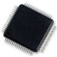
S9S12HY64J0MLH Freescale Semiconductor, S9S12HY64J0MLH Datasheet - Page 215

S9S12HY64J0MLH
Manufacturer Part Number
S9S12HY64J0MLH
Description
MCU 64K FLASH AUTO 64-LQFP
Manufacturer
Freescale Semiconductor
Series
HCS12r
Datasheet
1.S9S12HA32J0CLL.pdf
(792 pages)
Specifications of S9S12HY64J0MLH
Core Processor
HCS12
Core Size
16-Bit
Speed
32MHz
Connectivity
CAN, EBI/EMI, I²C, IrDA, LIN, SCI, SPI
Peripherals
LCD, Motor control PWM, POR, PWM, WDT
Number Of I /o
50
Program Memory Size
64KB (64K x 8)
Program Memory Type
FLASH
Eeprom Size
4K x 8
Ram Size
4K x 8
Voltage - Supply (vcc/vdd)
4.5 V ~ 5.5 V
Data Converters
A/D 6x10b
Oscillator Type
Internal
Operating Temperature
-40°C ~ 125°C
Package / Case
64-LQFP
Controller Family/series
S12
No. Of I/o's
50
Ram Memory Size
4KB
Cpu Speed
64MHz
No. Of Timers
2
Rohs Compliant
Yes
Processor Series
S12HY
Core
HCS12
3rd Party Development Tools
EWHCS12
Development Tools By Supplier
DEMO9S12HY64
Lead Free Status / RoHS Status
Lead free / RoHS Compliant
Available stocks
Company
Part Number
Manufacturer
Quantity
Price
Company:
Part Number:
S9S12HY64J0MLH
Manufacturer:
Freescale Semiconductor
Quantity:
10 000
- Current page: 215 of 792
- Download datasheet (4Mb)
Field2 Bits in Normal and Loop1 Modes
6.4.5.4
Freescale Semiconductor
PC17
PC16
CSD
CVA
Pure PC Mode
Bit
Compressed
3
2
1
0
Mode
Source Destination Indicator — In Normal and Loop1 mode this bit indicates if the corresponding stored
address is a source or destination address. This bit has no meaning in Compressed Pure PC mode.
0 Source Address
1 Destination Address
Vector Indicator — In Normal and Loop1 mode this bit indicates if the corresponding stored address is a vector
address. Vector addresses are destination addresses, thus if CVA is set, then the corresponding CSD is also set.
This bit has no meaning in Compressed Pure PC mode.
0 Non-Vector Destination Address
1 Vector Destination Address
Program Counter bit 17— In Normal and Loop1 mode this bit corresponds to program counter bit 17.
Program Counter bit 16— In Normal and Loop1 mode this bit corresponds to program counter bit 16.
Trace Buffer Organization (Compressed Pure PC mode)
Configured for end aligned triggering in compressed PurePC mode, then
after rollover it is possible that the oldest base address is overwritten. In this
case all entries between the pointer and the next base address have lost their
base address following rollover. For example in
rollover has occurred, Line 1, PC1, is overwritten with a new entry. Thus the
entries on Lines 2 and 3 have lost their base address. For reconstruction of
program flow the first base address following the pointer must be used, in
the example, Line 4. The pointer points to the oldest entry, Line 2.
Table 6-40. Trace Buffer Organization Example (Compressed PurePC mode)
Number
Line 1
Line 2
Line 3
Line 4
Line 5
Line 6
Line
Field 3
2-bits
00
11
01
00
10
00
MC9S12HY/HA-Family Reference Manual, Rev. 1.04
Table 6-39. PCH Field Descriptions
Figure 6-26. Information Bits PCH
CSD
Bit 3
Field 2
6-bits
PC4
0
0
Bit 2
CVA
NOTE
PC1 (Initial 18-bit PC Base Address)
PC6 (New 18-bit PC Base Address)
PC9 (New 18-bit PC Base Address)
Description
PC17
Bit 1
Table 6-40
Field 1
PC16
6-bits
Bit 0
PC3
PC8
0
if one line of
S12S Debug Module (S12SDBGV2)
Field 0
6-bits
PC2
PC5
PC7
215
Related parts for S9S12HY64J0MLH
Image
Part Number
Description
Manufacturer
Datasheet
Request
R
Part Number:
Description:
Manufacturer:
Freescale Semiconductor, Inc
Datasheet:
Part Number:
Description:
Manufacturer:
Freescale Semiconductor, Inc
Datasheet:
Part Number:
Description:
Manufacturer:
Freescale Semiconductor, Inc
Datasheet:
Part Number:
Description:
Manufacturer:
Freescale Semiconductor, Inc
Datasheet:
Part Number:
Description:
Manufacturer:
Freescale Semiconductor, Inc
Datasheet:
Part Number:
Description:
Manufacturer:
Freescale Semiconductor, Inc
Datasheet:
Part Number:
Description:
Manufacturer:
Freescale Semiconductor, Inc
Datasheet:
Part Number:
Description:
Manufacturer:
Freescale Semiconductor, Inc
Datasheet:
Part Number:
Description:
Manufacturer:
Freescale Semiconductor, Inc
Datasheet:
Part Number:
Description:
Manufacturer:
Freescale Semiconductor, Inc
Datasheet:
Part Number:
Description:
Manufacturer:
Freescale Semiconductor, Inc
Datasheet:
Part Number:
Description:
Manufacturer:
Freescale Semiconductor, Inc
Datasheet:
Part Number:
Description:
Manufacturer:
Freescale Semiconductor, Inc
Datasheet:
Part Number:
Description:
Manufacturer:
Freescale Semiconductor, Inc
Datasheet:
Part Number:
Description:
Manufacturer:
Freescale Semiconductor, Inc
Datasheet:


