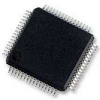
S9S12HY64J0MLH Freescale Semiconductor, S9S12HY64J0MLH Datasheet - Page 498

S9S12HY64J0MLH
Manufacturer Part Number
S9S12HY64J0MLH
Description
MCU 64K FLASH AUTO 64-LQFP
Manufacturer
Freescale Semiconductor
Series
HCS12r
Datasheet
1.S9S12HA32J0CLL.pdf
(792 pages)
Specifications of S9S12HY64J0MLH
Core Processor
HCS12
Core Size
16-Bit
Speed
32MHz
Connectivity
CAN, EBI/EMI, I²C, IrDA, LIN, SCI, SPI
Peripherals
LCD, Motor control PWM, POR, PWM, WDT
Number Of I /o
50
Program Memory Size
64KB (64K x 8)
Program Memory Type
FLASH
Eeprom Size
4K x 8
Ram Size
4K x 8
Voltage - Supply (vcc/vdd)
4.5 V ~ 5.5 V
Data Converters
A/D 6x10b
Oscillator Type
Internal
Operating Temperature
-40°C ~ 125°C
Package / Case
64-LQFP
Controller Family/series
S12
No. Of I/o's
50
Ram Memory Size
4KB
Cpu Speed
64MHz
No. Of Timers
2
Rohs Compliant
Yes
Processor Series
S12HY
Core
HCS12
3rd Party Development Tools
EWHCS12
Development Tools By Supplier
DEMO9S12HY64
Lead Free Status / RoHS Status
Lead free / RoHS Compliant
Available stocks
Company
Part Number
Manufacturer
Quantity
Price
Company:
Part Number:
S9S12HY64J0MLH
Manufacturer:
Freescale Semiconductor
Quantity:
10 000
- Current page: 498 of 792
- Download datasheet (4Mb)
Timer Module (TIM16B8CV2) Block Description
To operate the 16-bit pulse accumulator independently of input capture or output compare 7 and 0
respectively the user must set the corresponding bits IOSx = 1, OMx = 0 and OLx = 0. OC7M7 in the
OC7M register must also be cleared.
To enable output action using the OM7 and OL7 bits on the timer port,the corresponding bit OC7M7 in
the OC7M register must also be cleared. The settings for these bits can be seen in
Note: in
IOSx is the register TIOS bit x,
OC7Mx is the register OC7M bit x,
TCx is timer Input Capture/Output Compare register,
IOCx is channel x,
OMx/OLx is the register TCTL1/TCTL2,
OC7Dx is the register OC7D bit x.
IOCx = OC7Dx+ OMx/OLx, means that both OC7 event and OCx event will change channel x value.
14.3.2.9
498
Module Base + 0x000A
Module Base + 0x000B
IOCx=OC7Dx
IOC7=OM7/O
TC7=TCx
Reset
Reset
L7
W
W
R
R
Table
OC7Mx=1
EDG7B
EDG3B
Timer Control Register 3/Timer Control Register 4 (TCTL3 and TCTL4)
0
0
IOCx=OC7Dx
IOC7=OM7/O
7
7
14-10, the IOS7 and IOSx should be set to 1
+OMx/OLx
TC7>TCx
L7
OC7M7=0
EDG7A
EDG3A
0
0
6
6
TC7=TCx
Figure 14-16. Timer Control Register 3 (TCTL3)
Figure 14-17. Timer Control Register 4 (TCTL4)
MC9S12HY/HA-Family Reference Manual, Rev. 1.04
Table 14-10. The OC7 and OCx event priority
IOC7=OM7/OL7
IOCx=OMx/OLx
OC7Mx=0
EDG6B
EDG2B
0
0
5
5
TC7>TCx
EDG6A
EDG2A
0
0
4
4
IOC7=OC7D7
IOCx=OC7Dx
TC7=TCx
EDG5B
EDG1B
OC7Mx=1
0
0
3
3
IOC7=OC7D7
IOCx=OC7Dx
+OMx/OLx
TC7>TCx
EDG5A
EDG1A
OC7M7=1
0
0
2
2
TC7=TCx
Table 14-10
EDG4B
EDG0B
Freescale Semiconductor
IOCx=OMx/OLx
IOC7=OC7D7
0
0
1
1
OC7Mx=0
TC7>TCx
EDG4A
EDG0A
0
0
0
0
Related parts for S9S12HY64J0MLH
Image
Part Number
Description
Manufacturer
Datasheet
Request
R
Part Number:
Description:
Manufacturer:
Freescale Semiconductor, Inc
Datasheet:
Part Number:
Description:
Manufacturer:
Freescale Semiconductor, Inc
Datasheet:
Part Number:
Description:
Manufacturer:
Freescale Semiconductor, Inc
Datasheet:
Part Number:
Description:
Manufacturer:
Freescale Semiconductor, Inc
Datasheet:
Part Number:
Description:
Manufacturer:
Freescale Semiconductor, Inc
Datasheet:
Part Number:
Description:
Manufacturer:
Freescale Semiconductor, Inc
Datasheet:
Part Number:
Description:
Manufacturer:
Freescale Semiconductor, Inc
Datasheet:
Part Number:
Description:
Manufacturer:
Freescale Semiconductor, Inc
Datasheet:
Part Number:
Description:
Manufacturer:
Freescale Semiconductor, Inc
Datasheet:
Part Number:
Description:
Manufacturer:
Freescale Semiconductor, Inc
Datasheet:
Part Number:
Description:
Manufacturer:
Freescale Semiconductor, Inc
Datasheet:
Part Number:
Description:
Manufacturer:
Freescale Semiconductor, Inc
Datasheet:
Part Number:
Description:
Manufacturer:
Freescale Semiconductor, Inc
Datasheet:
Part Number:
Description:
Manufacturer:
Freescale Semiconductor, Inc
Datasheet:
Part Number:
Description:
Manufacturer:
Freescale Semiconductor, Inc
Datasheet:


