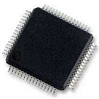
S9S12HY64J0MLH Freescale Semiconductor, S9S12HY64J0MLH Datasheet - Page 719

S9S12HY64J0MLH
Manufacturer Part Number
S9S12HY64J0MLH
Description
MCU 64K FLASH AUTO 64-LQFP
Manufacturer
Freescale Semiconductor
Series
HCS12r
Datasheet
1.S9S12HA32J0CLL.pdf
(792 pages)
Specifications of S9S12HY64J0MLH
Core Processor
HCS12
Core Size
16-Bit
Speed
32MHz
Connectivity
CAN, EBI/EMI, I²C, IrDA, LIN, SCI, SPI
Peripherals
LCD, Motor control PWM, POR, PWM, WDT
Number Of I /o
50
Program Memory Size
64KB (64K x 8)
Program Memory Type
FLASH
Eeprom Size
4K x 8
Ram Size
4K x 8
Voltage - Supply (vcc/vdd)
4.5 V ~ 5.5 V
Data Converters
A/D 6x10b
Oscillator Type
Internal
Operating Temperature
-40°C ~ 125°C
Package / Case
64-LQFP
Controller Family/series
S12
No. Of I/o's
50
Ram Memory Size
4KB
Cpu Speed
64MHz
No. Of Timers
2
Rohs Compliant
Yes
Processor Series
S12HY
Core
HCS12
3rd Party Development Tools
EWHCS12
Development Tools By Supplier
DEMO9S12HY64
Lead Free Status / RoHS Status
Lead free / RoHS Compliant
Available stocks
Company
Part Number
Manufacturer
Quantity
Price
Company:
Part Number:
S9S12HY64J0MLH
Manufacturer:
Freescale Semiconductor
Quantity:
10 000
- Current page: 719 of 792
- Download datasheet (4Mb)
A.1.5
Absolute maximum ratings are stress ratings only. A functional operation under or outside those maxima
is not guaranteed. Stress beyond those limits may affect the reliability or cause permanent damage of the
device.
This device contains circuitry protecting against damage due to high static voltage or electrical fields;
however, it is advised that normal precautions be taken to avoid application of any voltages higher than
maximum-rated voltages to this high-impedance circuit. Reliability of operation is enhanced if unused
inputs are tied to an appropriate logic voltage level (e.g., either V
1. Beyond absolute maximum ratings device might be damaged.
2. All digital I/O pins are internally clamped to V
A.1.6
All ESD testing is in conformity with CDF-AEC-Q100 stress test qualification for automotive grade
integrated circuits. During the device qualification ESD stresses were performed for the Human Body
Model (HBM) and the Charge Device Model.
A device will be defined as a failure if after exposure to ESD pulses the device no longer meets the device
specification. Complete DC parametric and functional testing is performed per the applicable device
specification at room temperature followed by hot temperature, unless specified otherwise in the device
specification.
Freescale Semiconductor
Num
10
11
12
13
1
2
3
4
5
6
7
8
9
I/O, regulator and analog supply voltage
Voltage difference V
Voltage difference V
Voltage difference V
Voltage difference V
Voltage difference V
Voltage difference V
Digital I/O input voltage
EXTAL, XTAL
Instantaneous maximum current
Instantaneous maximum current
Instantaneous maximum current
Storage temperature range
Single pin limit for all digital I/O pins
Single pin limit for all the power pins
Single pin limit for EXTAL, XTAL
Absolute Maximum Ratings
ESD Protection and Latch-up Immunity
DDX
SSX
DDX
SSX
DDM1,2
SSM1,2
to V
to V
to V
to V
MC9S12HY/HA-Family Reference Manual, Rev. 1.04
to V
to V
SSA
SSM1,2
DDA
DDM1,2
Table A-1. Absolute Maximum Ratings
Rating
SSA
DDA
SSX
(2)
and V
DDX
, or V
SSA
and V
DDA
SS35
Symbol
V
VDDXM
VSSXM
VDDMA
VSSMA
VDDXA
VSSXA
T stg
V
or V
V
DD35
I
I
I
DL
DL
ILV
D
IN
or V
(1)
SSM
DD35
and V
–0.3
–0.3
–0.3
–0.3
–0.3
–0.3
–0.3
–0.3
–0.3
Min
–25
–25
–65
-50
).
DDM
Electrical Characteristics
Max
2.16
+25
+50
+25
155
6.0
0.3
0.3
0.3
0.3
0.3
0.3
6.0
Unit
mA
mA
mA
V
V
V
V
V
V
V
V
V
C
719
Related parts for S9S12HY64J0MLH
Image
Part Number
Description
Manufacturer
Datasheet
Request
R
Part Number:
Description:
Manufacturer:
Freescale Semiconductor, Inc
Datasheet:
Part Number:
Description:
Manufacturer:
Freescale Semiconductor, Inc
Datasheet:
Part Number:
Description:
Manufacturer:
Freescale Semiconductor, Inc
Datasheet:
Part Number:
Description:
Manufacturer:
Freescale Semiconductor, Inc
Datasheet:
Part Number:
Description:
Manufacturer:
Freescale Semiconductor, Inc
Datasheet:
Part Number:
Description:
Manufacturer:
Freescale Semiconductor, Inc
Datasheet:
Part Number:
Description:
Manufacturer:
Freescale Semiconductor, Inc
Datasheet:
Part Number:
Description:
Manufacturer:
Freescale Semiconductor, Inc
Datasheet:
Part Number:
Description:
Manufacturer:
Freescale Semiconductor, Inc
Datasheet:
Part Number:
Description:
Manufacturer:
Freescale Semiconductor, Inc
Datasheet:
Part Number:
Description:
Manufacturer:
Freescale Semiconductor, Inc
Datasheet:
Part Number:
Description:
Manufacturer:
Freescale Semiconductor, Inc
Datasheet:
Part Number:
Description:
Manufacturer:
Freescale Semiconductor, Inc
Datasheet:
Part Number:
Description:
Manufacturer:
Freescale Semiconductor, Inc
Datasheet:
Part Number:
Description:
Manufacturer:
Freescale Semiconductor, Inc
Datasheet:


