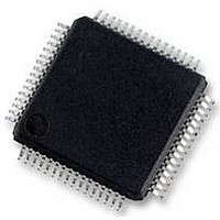
S9S12HY64J0MLH Freescale Semiconductor, S9S12HY64J0MLH Datasheet - Page 213

S9S12HY64J0MLH
Manufacturer Part Number
S9S12HY64J0MLH
Description
MCU 64K FLASH AUTO 64-LQFP
Manufacturer
Freescale Semiconductor
Series
HCS12r
Datasheet
1.S9S12HA32J0CLL.pdf
(792 pages)
Specifications of S9S12HY64J0MLH
Core Processor
HCS12
Core Size
16-Bit
Speed
32MHz
Connectivity
CAN, EBI/EMI, I²C, IrDA, LIN, SCI, SPI
Peripherals
LCD, Motor control PWM, POR, PWM, WDT
Number Of I /o
50
Program Memory Size
64KB (64K x 8)
Program Memory Type
FLASH
Eeprom Size
4K x 8
Ram Size
4K x 8
Voltage - Supply (vcc/vdd)
4.5 V ~ 5.5 V
Data Converters
A/D 6x10b
Oscillator Type
Internal
Operating Temperature
-40°C ~ 125°C
Package / Case
64-LQFP
Controller Family/series
S12
No. Of I/o's
50
Ram Memory Size
4KB
Cpu Speed
64MHz
No. Of Timers
2
Rohs Compliant
Yes
Processor Series
S12HY
Core
HCS12
3rd Party Development Tools
EWHCS12
Development Tools By Supplier
DEMO9S12HY64
Lead Free Status / RoHS Status
Lead free / RoHS Compliant
Available stocks
Company
Part Number
Manufacturer
Quantity
Price
Company:
Part Number:
S9S12HY64J0MLH
Manufacturer:
Freescale Semiconductor
Quantity:
10 000
- Current page: 213 of 792
- Download datasheet (4Mb)
6.4.5.2.2
Loop1 Mode, similarly to Normal Mode also stores only COF address information to the trace buffer, it
however allows the filtering out of redundant information.
The intent of Loop1 Mode is to prevent the Trace Buffer from being filled entirely with duplicate
information from a looping construct such as delays using the DBNE instruction or polling loops using
BRSET/BRCLR instructions. Immediately after address information is placed in the Trace Buffer, the
DBG module writes this value into a background register. This prevents consecutive duplicate address
entries in the Trace Buffer resulting from repeated branches.
Loop1 Mode only inhibits consecutive duplicate source address entries that would typically be stored in
most tight looping constructs. It does not inhibit repeated entries of destination addresses or vector
addresses, since repeated entries of these would most likely indicate a bug in the user’s code that the DBG
module is designed to help find.
6.4.5.2.3
In Detail Mode, address and data for all memory and register accesses is stored in the trace buffer. This
mode is intended to supply additional information on indexed, indirect addressing modes where storing
only the destination address would not provide all information required for a user to determine where the
code is in error. This mode also features information bit storage to the trace buffer, for each address byte
storage. The information bits indicate the size of access (word or byte) and the type of access (read or
write).
When tracing in Detail Mode, all cycles are traced except those when the CPU is either in a free or opcode
fetch cycle.
6.4.5.2.4
In Compressed Pure PC Mode, the PC addresses of all executed opcodes, including illegal opcodes are
stored. A compressed storage format is used to increase the effective depth of the trace buffer. This is
achieved by storing the lower order bits each time and using 2 information bits to indicate if a 64 byte
boundary has been crossed, in which case the full PC is stored.
Each Trace Buffer row consists of 2 information bits and 18 PC address bits
6.4.5.3
ADRH, ADRM, ADRL denote address high, middle and low byte respectively. The numerical suffix refers
to the tracing count. The information format for Loop1 and Normal modes is identical. In Detail mode, the
address and data for each entry are stored on consecutive lines, thus the maximum number of entries is 32.
In this case DBGCNT bits are incremented twice, once for the address line and once for the data line, on
Freescale Semiconductor
Trace Buffer Organization (Normal, Loop1, Detail modes)
Loop1 Mode
Detail Mode
Compressed Pure PC Mode
When tracing is terminated using forced breakpoints, latency in breakpoint
generation means that opcodes following the opcode causing the breakpoint
can be stored to the trace buffer. The number of opcodes is dependent on
program flow. This can be avoided by using tagged breakpoints.
MC9S12HY/HA-Family Reference Manual, Rev. 1.04
NOTE:
S12S Debug Module (S12SDBGV2)
213
Related parts for S9S12HY64J0MLH
Image
Part Number
Description
Manufacturer
Datasheet
Request
R
Part Number:
Description:
Manufacturer:
Freescale Semiconductor, Inc
Datasheet:
Part Number:
Description:
Manufacturer:
Freescale Semiconductor, Inc
Datasheet:
Part Number:
Description:
Manufacturer:
Freescale Semiconductor, Inc
Datasheet:
Part Number:
Description:
Manufacturer:
Freescale Semiconductor, Inc
Datasheet:
Part Number:
Description:
Manufacturer:
Freescale Semiconductor, Inc
Datasheet:
Part Number:
Description:
Manufacturer:
Freescale Semiconductor, Inc
Datasheet:
Part Number:
Description:
Manufacturer:
Freescale Semiconductor, Inc
Datasheet:
Part Number:
Description:
Manufacturer:
Freescale Semiconductor, Inc
Datasheet:
Part Number:
Description:
Manufacturer:
Freescale Semiconductor, Inc
Datasheet:
Part Number:
Description:
Manufacturer:
Freescale Semiconductor, Inc
Datasheet:
Part Number:
Description:
Manufacturer:
Freescale Semiconductor, Inc
Datasheet:
Part Number:
Description:
Manufacturer:
Freescale Semiconductor, Inc
Datasheet:
Part Number:
Description:
Manufacturer:
Freescale Semiconductor, Inc
Datasheet:
Part Number:
Description:
Manufacturer:
Freescale Semiconductor, Inc
Datasheet:
Part Number:
Description:
Manufacturer:
Freescale Semiconductor, Inc
Datasheet:


