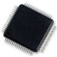
S9S12HY64J0MLH Freescale Semiconductor, S9S12HY64J0MLH Datasheet - Page 138

S9S12HY64J0MLH
Manufacturer Part Number
S9S12HY64J0MLH
Description
MCU 64K FLASH AUTO 64-LQFP
Manufacturer
Freescale Semiconductor
Series
HCS12r
Datasheet
1.S9S12HA32J0CLL.pdf
(792 pages)
Specifications of S9S12HY64J0MLH
Core Processor
HCS12
Core Size
16-Bit
Speed
32MHz
Connectivity
CAN, EBI/EMI, I²C, IrDA, LIN, SCI, SPI
Peripherals
LCD, Motor control PWM, POR, PWM, WDT
Number Of I /o
50
Program Memory Size
64KB (64K x 8)
Program Memory Type
FLASH
Eeprom Size
4K x 8
Ram Size
4K x 8
Voltage - Supply (vcc/vdd)
4.5 V ~ 5.5 V
Data Converters
A/D 6x10b
Oscillator Type
Internal
Operating Temperature
-40°C ~ 125°C
Package / Case
64-LQFP
Controller Family/series
S12
No. Of I/o's
50
Ram Memory Size
4KB
Cpu Speed
64MHz
No. Of Timers
2
Rohs Compliant
Yes
Processor Series
S12HY
Core
HCS12
3rd Party Development Tools
EWHCS12
Development Tools By Supplier
DEMO9S12HY64
Lead Free Status / RoHS Status
Lead free / RoHS Compliant
Available stocks
Company
Part Number
Manufacturer
Quantity
Price
Company:
Part Number:
S9S12HY64J0MLH
Manufacturer:
Freescale Semiconductor
Quantity:
10 000
- Current page: 138 of 792
- Download datasheet (4Mb)
S12P Memory Map Control (S12PMMCV1)
3.3.2
This section consists of the S12PMMC control register descriptions in address order.
3.3.2.1
Read: Anytime.
Write: Only if a transition is allowed (see
The MODC bit of the MODE register is used to select the MCU’s operating mode.
138
Address
Address: 0x000B
1. External signal (see
0x000B
0x0011
0x0015
Reset
MODC
Field
7
W
R
MODC
Register
DIRECT
MODC
PPAGE
Register Descriptions
MODE
Name
Mode Select Bit — This bit controls the current operating mode during RESET high (inactive). The external
mode pin MODC determines the operating mode during RESET low (active). The state of the pin is registered
into the respective register bit after the RESET signal goes inactive (see
Write restrictions exist to disallow transitions between certain modes.
changes. Attempting non authorized transitions will not change the MODE bit, but it will block further writes to
the register bit except in special modes.
Write accesses to the MODE register are blocked when the device is secured.
Mode Register (MODE)
7
1
Table
= Unimplemented or Reserved
W
W
W
R
R
R
3-3).
0
0
6
MODC
DP15
Bit 7
0
MC9S12HY/HA-Family Reference Manual, Rev. 1.04
Table 3-4. MODE Field Descriptions
Figure 3-2. MMC Register Summary
Figure 3-3. Mode Register (MODE)
= Unimplemented or Reserved
DP14
0
0
5
6
0
0
Figure
DP13
3-4).
5
0
0
0
0
4
Description
DP12
4
0
0
0
0
3
DP11
PIX3
3
0
Figure 3-4
Figure
0
0
2
DP10
PIX2
3-4).
2
0
illustrates all allowed mode
Freescale Semiconductor
0
0
1
PIX1
DP9
1
0
0
0
Bit 0
PIX0
0
DP8
0
Related parts for S9S12HY64J0MLH
Image
Part Number
Description
Manufacturer
Datasheet
Request
R
Part Number:
Description:
Manufacturer:
Freescale Semiconductor, Inc
Datasheet:
Part Number:
Description:
Manufacturer:
Freescale Semiconductor, Inc
Datasheet:
Part Number:
Description:
Manufacturer:
Freescale Semiconductor, Inc
Datasheet:
Part Number:
Description:
Manufacturer:
Freescale Semiconductor, Inc
Datasheet:
Part Number:
Description:
Manufacturer:
Freescale Semiconductor, Inc
Datasheet:
Part Number:
Description:
Manufacturer:
Freescale Semiconductor, Inc
Datasheet:
Part Number:
Description:
Manufacturer:
Freescale Semiconductor, Inc
Datasheet:
Part Number:
Description:
Manufacturer:
Freescale Semiconductor, Inc
Datasheet:
Part Number:
Description:
Manufacturer:
Freescale Semiconductor, Inc
Datasheet:
Part Number:
Description:
Manufacturer:
Freescale Semiconductor, Inc
Datasheet:
Part Number:
Description:
Manufacturer:
Freescale Semiconductor, Inc
Datasheet:
Part Number:
Description:
Manufacturer:
Freescale Semiconductor, Inc
Datasheet:
Part Number:
Description:
Manufacturer:
Freescale Semiconductor, Inc
Datasheet:
Part Number:
Description:
Manufacturer:
Freescale Semiconductor, Inc
Datasheet:
Part Number:
Description:
Manufacturer:
Freescale Semiconductor, Inc
Datasheet:


