HD6417144F50V Renesas Electronics America, HD6417144F50V Datasheet - Page 24
HD6417144F50V
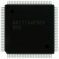
Manufacturer Part Number
HD6417144F50V
Description
IC SUPERH MCU ROMLESS 112QFP
Manufacturer
Renesas Electronics America
Series
SuperH® SH7144r
Datasheet
1.HD64F7144F50V.pdf
(932 pages)
Specifications of HD6417144F50V
Core Processor
SH-2
Core Size
32-Bit
Speed
50MHz
Connectivity
EBI/EMI, I²C, SCI
Peripherals
DMA, POR, PWM, WDT
Number Of I /o
74
Program Memory Type
ROMless
Ram Size
8K x 8
Voltage - Supply (vcc/vdd)
3 V ~ 3.6 V
Data Converters
A/D 8x10b
Oscillator Type
Internal
Operating Temperature
-20°C ~ 75°C
Package / Case
112-QFP
For Use With
HS0005KCU11H - EMULATOR E10A-USB H8S(X),SH2(A)EDK7145 - DEV EVALUATION KIT SH7145
Lead Free Status / RoHS Status
Lead free / RoHS Compliant
Eeprom Size
-
Program Memory Size
-
Available stocks
Company
Part Number
Manufacturer
Quantity
Price
Company:

Part Number:
HD6417144F50V
Manufacturer:
Renesas Electronics America
Quantity:
10 000


Section 23 Advanced User Debugger (AUD) ...................................................705
23.1 Overview........................................................................................................................... 705
23.2 Input/Output Pins .............................................................................................................. 707
23.3 Branch Trace Mode........................................................................................................... 710
23.4 RAM Monitor Mode ......................................................................................................... 712
23.5 Usage Notes ...................................................................................................................... 715
Section 24 Power-Down Modes ........................................................................719
24.1 Input/Output Pins .............................................................................................................. 721
24.2 Register Descriptions ........................................................................................................ 721
24.3 Operation .......................................................................................................................... 727
24.4 Usage Notes ...................................................................................................................... 731
Rev.4.00 Mar. 27, 2008 Page xxii of xliv
REJ09B0108-0400
23.1.1 Features................................................................................................................ 705
23.1.2 Block Diagram..................................................................................................... 706
23.2.1 Pin Descriptions................................................................................................... 707
23.3.1 Overview.............................................................................................................. 710
23.3.2 Operation ............................................................................................................. 710
23.4.1 Overview.............................................................................................................. 712
23.4.2 Communication Protocol ..................................................................................... 712
23.4.3 Operation ............................................................................................................. 713
23.5.1 Initialization ......................................................................................................... 715
23.5.2 Operation in Software Standby Mode.................................................................. 715
23.5.3 Setting the PA15/CK pin ..................................................................................... 715
23.5.4 Pin States ............................................................................................................. 716
23.5.5 AUD Start-up Sequence....................................................................................... 716
23.5.6 RAM Monitor Operation Using the PD22/AUDCK Pin ..................................... 716
23.5.7 Settings of AUD-Related Pins when Using E10A ............................................... 717
24.2.1 Standby Control Register (SBYCR) .................................................................... 722
24.2.2 System Control Register (SYSCR) ...................................................................... 724
24.2.3 Module Standby Control Register 1 and 2 (MSTCR1 and MSTCR2)................. 725
24.3.1 Sleep Mode .......................................................................................................... 727
24.3.2 Software Standby Mode....................................................................................... 728
24.3.3 Module Standby Mode......................................................................................... 730
24.4.1 I/O Port Status...................................................................................................... 731
24.4.2 Current Consumption during Oscillation Stabilization Wait Period.................... 731
24.4.3 On-Chip Peripheral Module Interrupt.................................................................. 731
24.4.4 Writing to MSTCR1 and MSTCR2 ..................................................................... 731
24.4.5 DMAC, DTC, or AUD Operation in Sleep Mode................................................ 731
Related parts for HD6417144F50V
Image
Part Number
Description
Manufacturer
Datasheet
Request
R

Part Number:
Description:
KIT STARTER FOR M16C/29
Manufacturer:
Renesas Electronics America
Datasheet:

Part Number:
Description:
KIT STARTER FOR R8C/2D
Manufacturer:
Renesas Electronics America
Datasheet:

Part Number:
Description:
R0K33062P STARTER KIT
Manufacturer:
Renesas Electronics America
Datasheet:

Part Number:
Description:
KIT STARTER FOR R8C/23 E8A
Manufacturer:
Renesas Electronics America
Datasheet:

Part Number:
Description:
KIT STARTER FOR R8C/25
Manufacturer:
Renesas Electronics America
Datasheet:

Part Number:
Description:
KIT STARTER H8S2456 SHARPE DSPLY
Manufacturer:
Renesas Electronics America
Datasheet:

Part Number:
Description:
KIT STARTER FOR R8C38C
Manufacturer:
Renesas Electronics America
Datasheet:

Part Number:
Description:
KIT STARTER FOR R8C35C
Manufacturer:
Renesas Electronics America
Datasheet:

Part Number:
Description:
KIT STARTER FOR R8CL3AC+LCD APPS
Manufacturer:
Renesas Electronics America
Datasheet:
Part Number:
Description:
KIT STARTER FOR RX610
Manufacturer:
Renesas Electronics America
Datasheet:

Part Number:
Description:
KIT STARTER FOR R32C/118
Manufacturer:
Renesas Electronics America
Datasheet:

Part Number:
Description:
KIT DEV RSK-R8C/26-29
Manufacturer:
Renesas Electronics America
Datasheet:

Part Number:
Description:
KIT STARTER FOR SH7124
Manufacturer:
Renesas Electronics America
Datasheet:

Part Number:
Description:
KIT STARTER FOR H8SX/1622
Manufacturer:
Renesas Electronics America
Datasheet:

Part Number:
Description:
KIT DEV FOR SH7203
Manufacturer:
Renesas Electronics America
Datasheet: