HD6417144F50V Renesas Electronics America, HD6417144F50V Datasheet - Page 43
HD6417144F50V
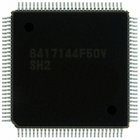
Manufacturer Part Number
HD6417144F50V
Description
IC SUPERH MCU ROMLESS 112QFP
Manufacturer
Renesas Electronics America
Series
SuperH® SH7144r
Datasheet
1.HD64F7144F50V.pdf
(932 pages)
Specifications of HD6417144F50V
Core Processor
SH-2
Core Size
32-Bit
Speed
50MHz
Connectivity
EBI/EMI, I²C, SCI
Peripherals
DMA, POR, PWM, WDT
Number Of I /o
74
Program Memory Type
ROMless
Ram Size
8K x 8
Voltage - Supply (vcc/vdd)
3 V ~ 3.6 V
Data Converters
A/D 8x10b
Oscillator Type
Internal
Operating Temperature
-20°C ~ 75°C
Package / Case
112-QFP
For Use With
HS0005KCU11H - EMULATOR E10A-USB H8S(X),SH2(A)EDK7145 - DEV EVALUATION KIT SH7145
Lead Free Status / RoHS Status
Lead free / RoHS Compliant
Eeprom Size
-
Program Memory Size
-
Available stocks
Company
Part Number
Manufacturer
Quantity
Price
Company:

Part Number:
HD6417144F50V
Manufacturer:
Renesas Electronics America
Quantity:
10 000


Table 11.13
Table 11.14
Table 11.15
Table 11.16
Table 11.17
Table 11.18
Table 11.19
Table 11.20
Table 11.21
Table 11.22
Table 11.23
Table 11.24
Table 11.25
Table 11.26
Table 11.27
Table 11.28
Table 11.29
Table 11.30
Table 11.31
Table 11.32
Table 11.33
Table 11.34
Table 11.35
Table 11.36
Table 11.37
Table 11.38
Table 11.39
Table 11.40
Table 11.41
Table 11.42
Table 11.43
Table 11.44
Table 11.45
Section 12 Watchdog Timer (WDT)
Table 12.1
Table 12.2
Section 13 Serial Communication Interface (SCI)
Table 13.1
Table 13.2
TIOR_2 (Channel 2) .............................................................................................231
TIORH_3 (Channel 3) ..........................................................................................232
TIORL_3 (Channel 3)...........................................................................................233
TIORH_4 (Channel 4) ..........................................................................................234
TIORL_4 (Channel 4)...........................................................................................235
TIORH_0 (Channel 0) ..........................................................................................236
TIORL_0 (Channel 0)...........................................................................................237
TIOR_1 (Channel 1) .............................................................................................238
TIOR_2 (Channel 2) .............................................................................................239
TIORH_3 (Channel 3) ..........................................................................................240
TIORL_3 (Channel 3)...........................................................................................241
TIORH_4 (Channel 4) ..........................................................................................242
TIORL_4 (Channel 4)...........................................................................................243
Output Level Select Function ...............................................................................253
Output Level Select Function ...............................................................................254
Output level Select Function.................................................................................256
Register Combinations in Buffer Operation .........................................................266
Cascaded Combinations........................................................................................269
PWM Output Registers and Output Pins ..............................................................272
Phase Counting Mode Clock Input Pins ...............................................................276
Up/Down-Count Conditions in Phase Counting Mode 1......................................277
Up/Down-Count Conditions in Phase Counting Mode 2......................................278
Up/Down-Count Conditions in Phase Counting Mode 3......................................279
Up/Down-Count Conditions in Phase Counting Mode 4......................................280
Output Pins for Reset-Synchronized PWM Mode ................................................282
Register Settings for Reset-Synchronized PWM Mode ........................................282
Output Pins for Complementary PWM Mode.......................................................285
Register Settings for Complementary PWM Mode ..............................................286
Registers and Counters Requiring Initialization ...................................................293
MTU Interrupts .....................................................................................................311
Mode Transition Combinations ............................................................................337
Pin Configuration..................................................................................................370
Pin Combinations..................................................................................................370
Pin Configuration..................................................................................................380
WDT Interrupt Source (in Interval Timer Mode) .................................................388
Pin Configuration..................................................................................................395
Relationships between N Setting in BRR and Effective Bit Rate B
Rev.4.00 Mar. 27, 2008, Page xli of xliv
REJ09B0108-0400
0
....................416
Related parts for HD6417144F50V
Image
Part Number
Description
Manufacturer
Datasheet
Request
R

Part Number:
Description:
KIT STARTER FOR M16C/29
Manufacturer:
Renesas Electronics America
Datasheet:

Part Number:
Description:
KIT STARTER FOR R8C/2D
Manufacturer:
Renesas Electronics America
Datasheet:

Part Number:
Description:
R0K33062P STARTER KIT
Manufacturer:
Renesas Electronics America
Datasheet:

Part Number:
Description:
KIT STARTER FOR R8C/23 E8A
Manufacturer:
Renesas Electronics America
Datasheet:

Part Number:
Description:
KIT STARTER FOR R8C/25
Manufacturer:
Renesas Electronics America
Datasheet:

Part Number:
Description:
KIT STARTER H8S2456 SHARPE DSPLY
Manufacturer:
Renesas Electronics America
Datasheet:

Part Number:
Description:
KIT STARTER FOR R8C38C
Manufacturer:
Renesas Electronics America
Datasheet:

Part Number:
Description:
KIT STARTER FOR R8C35C
Manufacturer:
Renesas Electronics America
Datasheet:

Part Number:
Description:
KIT STARTER FOR R8CL3AC+LCD APPS
Manufacturer:
Renesas Electronics America
Datasheet:
Part Number:
Description:
KIT STARTER FOR RX610
Manufacturer:
Renesas Electronics America
Datasheet:

Part Number:
Description:
KIT STARTER FOR R32C/118
Manufacturer:
Renesas Electronics America
Datasheet:

Part Number:
Description:
KIT DEV RSK-R8C/26-29
Manufacturer:
Renesas Electronics America
Datasheet:

Part Number:
Description:
KIT STARTER FOR SH7124
Manufacturer:
Renesas Electronics America
Datasheet:

Part Number:
Description:
KIT STARTER FOR H8SX/1622
Manufacturer:
Renesas Electronics America
Datasheet:

Part Number:
Description:
KIT DEV FOR SH7203
Manufacturer:
Renesas Electronics America
Datasheet: