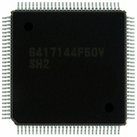
HD6417144F50V Renesas Electronics America, HD6417144F50V Datasheet - Page 355

HD6417144F50V
Manufacturer Part Number
HD6417144F50V
Description
IC SUPERH MCU ROMLESS 112QFP
Manufacturer
Renesas Electronics America
Series
SuperH® SH7144r
Datasheet
1.HD64F7144F50V.pdf
(932 pages)
Specifications of HD6417144F50V
Core Processor
SH-2
Core Size
32-Bit
Speed
50MHz
Connectivity
EBI/EMI, I²C, SCI
Peripherals
DMA, POR, PWM, WDT
Number Of I /o
74
Program Memory Type
ROMless
Ram Size
8K x 8
Voltage - Supply (vcc/vdd)
3 V ~ 3.6 V
Data Converters
A/D 8x10b
Oscillator Type
Internal
Operating Temperature
-20°C ~ 75°C
Package / Case
112-QFP
For Use With
HS0005KCU11H - EMULATOR E10A-USB H8S(X),SH2(A)EDK7145 - DEV EVALUATION KIT SH7145
Lead Free Status / RoHS Status
Lead free / RoHS Compliant
Eeprom Size
-
Program Memory Size
-
Available stocks
Company
Part Number
Manufacturer
Quantity
Price
Company:
Part Number:
HD6417144F50V
Manufacturer:
Renesas Electronics America
Quantity:
10 000
- Current page: 355 of 932
- Download datasheet (6Mb)
Complementary PWM Mode Output Protection Function:
Complementary PWM mode output has the following protection functions.
1. Register and counter miswrite prevention function
2. Halting of PWM output by external signal
3. Halting of PWM output when oscillator is stopped
With the exception of the buffer registers, which can be rewritten at any time, access by the
CPU can be enabled or disabled for the mode registers, control registers, compare registers,
and counters used in complementary PWM mode by means of the MTURWE bit in the bus
controller’s bus control register 1 (BCR1). The applicable registers are some (21 in total) of the
registers in channels 3 and 4 shown in the following:
⎯
This function enables miswriting due to CPU runaway to be prevented by disabling CPU
access to the mode registers, control registers, and counters. When the applicable registers are
read in the access-disabled state, undefined values are returned. Writing to these registers is
ignored.
The 6-phase PWM output pins can be set automatically to the high-impedance state by
inputting specified external signals. There are four external signal input pins.
See section 11.9, Port Output Enable (POE), for details.
If it is detected that the clock input to this LSI has stopped, the 6-phase PWM output pins
automatically go to the high-impedance state. The pin states are not guaranteed when the clock
is restarted.
See section 4.2, Function for Detecting Oscillator Halt.
TIORL_4, TIER_3 and TIER_4, TCNT_3 and TCNT_4, TGRA_3 and TGRA_4, TGRB_3
and TGRB_4, TOER, TOCR, TGCR, TCDR, and TDDR.
TCR_3 and TCR_4, TMDR_3 and TMDR_4, TIORH_3 and TIORH_4, TIORL_3 and
11.
Rev.4.00 Mar. 27, 2008 Page 309 of 882
Multi-Function Timer Pulse Unit (MTU)
REJ09B0108-0400
Related parts for HD6417144F50V
Image
Part Number
Description
Manufacturer
Datasheet
Request
R

Part Number:
Description:
KIT STARTER FOR M16C/29
Manufacturer:
Renesas Electronics America
Datasheet:

Part Number:
Description:
KIT STARTER FOR R8C/2D
Manufacturer:
Renesas Electronics America
Datasheet:

Part Number:
Description:
R0K33062P STARTER KIT
Manufacturer:
Renesas Electronics America
Datasheet:

Part Number:
Description:
KIT STARTER FOR R8C/23 E8A
Manufacturer:
Renesas Electronics America
Datasheet:

Part Number:
Description:
KIT STARTER FOR R8C/25
Manufacturer:
Renesas Electronics America
Datasheet:

Part Number:
Description:
KIT STARTER H8S2456 SHARPE DSPLY
Manufacturer:
Renesas Electronics America
Datasheet:

Part Number:
Description:
KIT STARTER FOR R8C38C
Manufacturer:
Renesas Electronics America
Datasheet:

Part Number:
Description:
KIT STARTER FOR R8C35C
Manufacturer:
Renesas Electronics America
Datasheet:

Part Number:
Description:
KIT STARTER FOR R8CL3AC+LCD APPS
Manufacturer:
Renesas Electronics America
Datasheet:

Part Number:
Description:
KIT STARTER FOR RX610
Manufacturer:
Renesas Electronics America
Datasheet:

Part Number:
Description:
KIT STARTER FOR R32C/118
Manufacturer:
Renesas Electronics America
Datasheet:

Part Number:
Description:
KIT DEV RSK-R8C/26-29
Manufacturer:
Renesas Electronics America
Datasheet:

Part Number:
Description:
KIT STARTER FOR SH7124
Manufacturer:
Renesas Electronics America
Datasheet:

Part Number:
Description:
KIT STARTER FOR H8SX/1622
Manufacturer:
Renesas Electronics America
Datasheet:

Part Number:
Description:
KIT DEV FOR SH7203
Manufacturer:
Renesas Electronics America
Datasheet:


