HD6417144F50V Renesas Electronics America, HD6417144F50V Datasheet - Page 510
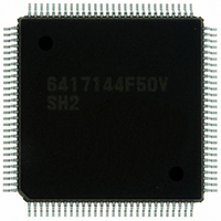
HD6417144F50V
Manufacturer Part Number
HD6417144F50V
Description
IC SUPERH MCU ROMLESS 112QFP
Manufacturer
Renesas Electronics America
Series
SuperH® SH7144r
Datasheet
1.HD64F7144F50V.pdf
(932 pages)
Specifications of HD6417144F50V
Core Processor
SH-2
Core Size
32-Bit
Speed
50MHz
Connectivity
EBI/EMI, I²C, SCI
Peripherals
DMA, POR, PWM, WDT
Number Of I /o
74
Program Memory Type
ROMless
Ram Size
8K x 8
Voltage - Supply (vcc/vdd)
3 V ~ 3.6 V
Data Converters
A/D 8x10b
Oscillator Type
Internal
Operating Temperature
-20°C ~ 75°C
Package / Case
112-QFP
For Use With
HS0005KCU11H - EMULATOR E10A-USB H8S(X),SH2(A)EDK7145 - DEV EVALUATION KIT SH7145
Lead Free Status / RoHS Status
Lead free / RoHS Compliant
Eeprom Size
-
Program Memory Size
-
Available stocks
Company
Part Number
Manufacturer
Quantity
Price
Company:

Part Number:
HD6417144F50V
Manufacturer:
Renesas Electronics America
Quantity:
10 000


13. Serial Communication Interface (SCI)
When the TE bit is cleared to 0, the transmission section is initialized regardless of the present
transmission status.
13.9.5
Transmission cannot be started when a receive error flag (ORER, PER, or FER) is set to 1, even if
the TDRE flag is cleared to 0. Be sure to clear the receive error flags to 0 before starting
transmission. Note also that receive error flags cannot be cleared to 0 even if the RE bit is cleared
to 0.
13.9.6
1. When using an external clock source for the serial clock, update TDR with the DMAC or the
2. Before reading the receive data register (RDR) with the DMAC or the DTC, select the receive-
13.9.7
1. Set TE = RE = 1 only when external clock SCK is 1.
2. Do not set TE = RE = 1 until at least four Pφ clocks after external clock SCK has changed
3. When receiving, RDRF is 1 when RE is cleared to 0 after 2.5 to 3.5 Pφ clocks from the rising
Rev.4.00 Mar. 27, 2008 Page 464 of 882
REJ09B0108-0400
DTC, and then after the elapse of five peripheral clocks (Pφ) or more, input a transmit clock. If
a transmit clock is input in the first four Pφ clocks after TDR is written, an error may occur
(figure 13.30).
data-full (RXI) interrupt of the SCI as a start-up source.
from 0 to 1.
edge of the RxD D7 bit SCK input, but copying to RDR is not possible.
Figure 13.30 Example of Clocked Synchronous Transmission with DMAC/DTC
Receive Error Flags and Transmit Operations (Clocked Synchronous Mode Only)
Notes on DMAC and DTC Use
Notes on Clocked Synchronous External Clock Mode
Note: During external clock operation, an error may occur if t is 4 Pφ clocks or less.
SCK
TDRE
t
D0
D1
D2
D3
D4
D5
D6
D7
Related parts for HD6417144F50V
Image
Part Number
Description
Manufacturer
Datasheet
Request
R

Part Number:
Description:
KIT STARTER FOR M16C/29
Manufacturer:
Renesas Electronics America
Datasheet:

Part Number:
Description:
KIT STARTER FOR R8C/2D
Manufacturer:
Renesas Electronics America
Datasheet:

Part Number:
Description:
R0K33062P STARTER KIT
Manufacturer:
Renesas Electronics America
Datasheet:

Part Number:
Description:
KIT STARTER FOR R8C/23 E8A
Manufacturer:
Renesas Electronics America
Datasheet:

Part Number:
Description:
KIT STARTER FOR R8C/25
Manufacturer:
Renesas Electronics America
Datasheet:

Part Number:
Description:
KIT STARTER H8S2456 SHARPE DSPLY
Manufacturer:
Renesas Electronics America
Datasheet:

Part Number:
Description:
KIT STARTER FOR R8C38C
Manufacturer:
Renesas Electronics America
Datasheet:

Part Number:
Description:
KIT STARTER FOR R8C35C
Manufacturer:
Renesas Electronics America
Datasheet:

Part Number:
Description:
KIT STARTER FOR R8CL3AC+LCD APPS
Manufacturer:
Renesas Electronics America
Datasheet:
Part Number:
Description:
KIT STARTER FOR RX610
Manufacturer:
Renesas Electronics America
Datasheet:

Part Number:
Description:
KIT STARTER FOR R32C/118
Manufacturer:
Renesas Electronics America
Datasheet:

Part Number:
Description:
KIT DEV RSK-R8C/26-29
Manufacturer:
Renesas Electronics America
Datasheet:

Part Number:
Description:
KIT STARTER FOR SH7124
Manufacturer:
Renesas Electronics America
Datasheet:

Part Number:
Description:
KIT STARTER FOR H8SX/1622
Manufacturer:
Renesas Electronics America
Datasheet:

Part Number:
Description:
KIT DEV FOR SH7203
Manufacturer:
Renesas Electronics America
Datasheet: