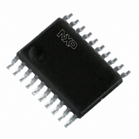
PCA9665PW,118 NXP Semiconductors, PCA9665PW,118 Datasheet - Page 12

PCA9665PW,118
Manufacturer Part Number
PCA9665PW,118
Description
IC CNTRLR PARALLEL/I2C 20TSSOP
Manufacturer
NXP Semiconductors
Datasheet
1.PCA9665D118.pdf
(90 pages)
Specifications of PCA9665PW,118
Package / Case
20-TSSOP
Controller Type
I²C Bus Controller
Interface
I²C
Voltage - Supply
2.3 V ~ 3.6 V
Current - Supply
100µA
Operating Temperature
-40°C ~ 85°C
Mounting Type
Surface Mount
Maximum Operating Temperature
+ 85 C
Minimum Operating Temperature
- 40 C
Mounting Style
SMD/SMT
Lead Free Status / RoHS Status
Lead free / RoHS Compliant
Lead Free Status / RoHS Status
Lead free / RoHS Compliant, Lead free / RoHS Compliant
Other names
568-4070-2
935279244118
PCA9665PW-T
PCA9665PW-T
935279244118
PCA9665PW-T
PCA9665PW-T
NXP Semiconductors
PCA9665_3
Product data sheet
7.3.2.1 The Byte Count register, I2CCOUNT (indirect address 00h)
7.3.2.2 The Own Address register, I2CADR (indirect address 01h)
7.3.2 Indirect registers
The I2CCOUNT register is an 8-bit read/write register. It contains the number of bytes that
have been stored in Master/Slave Buffered Receiver mode, and the number of bytes to be
sent in Master/Slave Buffered Transmitter mode. Bit 7 is the last byte control bit and
applies to the Master/Slave Buffered Receiver mode only. The data in the I2CCOUNT
register is relevant only in Buffered mode (MODE = 1) and should not be used (read or
written) in Byte mode (MODE = 0).
Table 13.
Table 14.
I2CADR is an 8-bit read/write register. It is not affected by the bus controller hardware.
The content of this register is unused when the controller is in a master mode. A master
should never transmit its own slave address. In the slave modes, the seven most
significant bits must be loaded with the microcontroller's own slave address and the least
significant bit determines if the General Call address will be recognized or not.
Remark: AD[7:1] must be different from the General Call address (000 0000) for proper
device operation.
Remark: The I2CADR default value is E0h.
Table 15.
Table 16.
Bit
7
6:0
Bit
7:1
0
AD7
LB
7
7
Symbol
LB
BC[6:0]
Symbol
AD[7:1]
GC
I2CCOUNT - Byte Count register (indirect address 00h) bit allocation
I2CCOUNT - Byte Count register (indirect address 00h) bit description
I2CADR - Address register (indirect address 01h) bit allocation
I2CADR - Address register (indirect address 01h) bit description
BC6
AD6
6
6
Description
Last Byte control bit. Master/Slave Buffered Receiver mode only.
Number of bytes to be read or written (up to 68 bytes). If BC[6:0] is equal to 0 or
greater than 68 (44h), no bytes will be read or written and an interrupt is
immediately generated after writing to the I2CCON register (in Buffered mode
only).
Description
Own slave address. The most significant bit corresponds to the first bit received
from the I
HIGH level on the I
General Call.
LB = 1: PCA9665 does not acknowledge the last received byte.
LB = 0: PCA9665 acknowledges the last received byte. A future bus
transaction must complete the read sequence by not acknowledging the last
byte.
GC = 1: General Call address (00h) is recognized.
GC = 0: General Call address (00h) is ignored.
Rev. 03 — 12 August 2008
2
BC5
AD5
C-bus after a START condition. A logic 1 in I2CADR corresponds to a
5
5
2
C-bus, and a logic 0 corresponds to a LOW level on the bus.
BC4
AD4
4
4
BC3
AD3
Fm+ parallel bus to I
3
3
BC2
AD2
2
2
PCA9665
BC1
AD1
© NXP B.V. 2008. All rights reserved.
2
1
1
C-bus controller
BC0
GC
12 of 90
0
0


