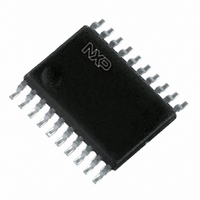
PCA9665PW,118 NXP Semiconductors, PCA9665PW,118 Datasheet - Page 9

PCA9665PW,118
Manufacturer Part Number
PCA9665PW,118
Description
IC CNTRLR PARALLEL/I2C 20TSSOP
Manufacturer
NXP Semiconductors
Datasheet
1.PCA9665D118.pdf
(90 pages)
Specifications of PCA9665PW,118
Package / Case
20-TSSOP
Controller Type
I²C Bus Controller
Interface
I²C
Voltage - Supply
2.3 V ~ 3.6 V
Current - Supply
100µA
Operating Temperature
-40°C ~ 85°C
Mounting Type
Surface Mount
Maximum Operating Temperature
+ 85 C
Minimum Operating Temperature
- 40 C
Mounting Style
SMD/SMT
Lead Free Status / RoHS Status
Lead free / RoHS Compliant
Lead Free Status / RoHS Status
Lead free / RoHS Compliant, Lead free / RoHS Compliant
Other names
568-4070-2
935279244118
PCA9665PW-T
PCA9665PW-T
935279244118
PCA9665PW-T
PCA9665PW-T
NXP Semiconductors
PCA9665_3
Product data sheet
7.3.1.4 The Control register, I2CCON (A1 = 1, A0 = 1)
In Byte mode, the CPU can read or write a single byte at a time. In Buffered mode, the
CPU can read or write up to 68 bytes at a time. See
more detail.
Remark: The I2CDAT register will capture the serial address as data when addressed via
the serial bus.
Remark: In Byte mode only, the data register will capture data from the serial bus during
38h (arbitration lost in slave address + R/W or data bytes causing this data in I2CDAT to
be changed), so the I2CDAT register will need to be reloaded when the bus becomes free.
In Buffered mode, the data is not written in the data register when arbitration is lost, which
keeps the buffer intact.
Table 9.
Table 10.
I2CCON is an 8-bit read/write register. Two bits are affected by the bus controller
hardware: the SI bit is set when a serial interrupt is requested, and the STO bit is cleared
when a STOP condition is present on the I
parallel interface automatically clears the SI bit, which causes the Serial Interrupt line to
be de-asserted and the next clock pulse on the SCL line to be generated.
Remark: Since none of the registers should be written to via the parallel interface once
the Serial Interrupt line has been de-asserted, all the other registers that need to be
modified should be written to before the content of the I2CCON register is modified.
Table 11.
Bit
7:0
SD7
AA
7
7
Symbol
SD[7:0]
I2CDAT - Data register (A1 = 0, A0 = 1) bit allocation
I2CDAT - Data register (A1 = 0, A0 = 1) bit description
I2CCON - Control register (A1 = 1, A0 = 1) bit allocation
ENSIO
SD6
6
6
Description
Eight bits to be transmitted or just received. A logic 1 in I2CDAT corresponds to
a HIGH level on the I
Rev. 03 — 12 August 2008
SD5
STA
5
5
2
STO
SD4
C-bus. A logic 0 corresponds to a LOW level on the bus.
4
4
2
C-bus. A Write to the I2CCON register via the
SD3
SI
Fm+ parallel bus to I
3
3
Section 8.1 “Configuration modes”
SD2
2
2
-
PCA9665
SD1
© NXP B.V. 2008. All rights reserved.
2
1
1
C-bus controller
-
MODE
SD0
0
0
9 of 90
for


