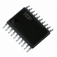
PCA9665PW,118 NXP Semiconductors, PCA9665PW,118 Datasheet - Page 16

PCA9665PW,118
Manufacturer Part Number
PCA9665PW,118
Description
IC CNTRLR PARALLEL/I2C 20TSSOP
Manufacturer
NXP Semiconductors
Datasheet
1.PCA9665D118.pdf
(90 pages)
Specifications of PCA9665PW,118
Package / Case
20-TSSOP
Controller Type
I²C Bus Controller
Interface
I²C
Voltage - Supply
2.3 V ~ 3.6 V
Current - Supply
100µA
Operating Temperature
-40°C ~ 85°C
Mounting Type
Surface Mount
Maximum Operating Temperature
+ 85 C
Minimum Operating Temperature
- 40 C
Mounting Style
SMD/SMT
Lead Free Status / RoHS Status
Lead free / RoHS Compliant
Lead Free Status / RoHS Status
Lead free / RoHS Compliant, Lead free / RoHS Compliant
Other names
568-4070-2
935279244118
PCA9665PW-T
PCA9665PW-T
935279244118
PCA9665PW-T
PCA9665PW-T
NXP Semiconductors
8. PCA9665 modes
PCA9665_3
Product data sheet
8.1.1 Byte mode
8.1.2 Buffered mode
8.1 Configuration modes
8.2 Operating modes
Byte mode and Buffered mode are selected using the MODE bit in I2CCON register:
The Byte mode allows communication on a single command basis. Only one specific
command is executed at a time and the Status Register is updated once this single
command has been performed. A command can be a START, a STOP, a Byte Write, a
Byte Read, and so on.
The Buffered mode allows several instructions to be executed before an Interrupt is
generated and before the I2CSTA register is updated. This allows the microcontroller to
request a sequence, up to 68 bytes in a single transmission and lets the PCA9665
perform it without having to access the Status Register and the Control Register each time
a single command is performed. The microcontroller can then perform other tasks while
the PCA9665 performs the requested sequence.
The number of bytes that needs to be sent from the internal buffer (Transmitter mode) or
received into the internal buffer (Receiver mode) is defined in the indirectly addressed
I2CCOUNT Register (BC[6:0]). Up to 68 bytes can be sent or received.
The four operating modes are:
Each mode can be used on a byte basis (Byte mode) or in an up to 68-byte buffer basis
(Buffered mode).
Data transfers in each mode of operation are shown in
figures contain the following abbreviations:
S — START condition
SLA — 7-bit slave address
R — Read bit (HIGH level at SDA)
W — Write bit (LOW level at SDA)
A — Acknowledge bit (LOW level at SDA)
A — Not acknowledge bit (HIGH level at SDA)
Data — 8-bit data byte
•
•
•
•
MODE = 0: Byte mode
MODE = 1: Buffered mode
Master Transmitter
Master Receiver
Slave Receiver
Slave Transmitter
Rev. 03 — 12 August 2008
Fm+ parallel bus to I
Figure 7
through
PCA9665
© NXP B.V. 2008. All rights reserved.
2
Figure
C-bus controller
10. These
16 of 90


