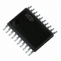
PCA9665PW,118 NXP Semiconductors, PCA9665PW,118 Datasheet - Page 53

PCA9665PW,118
Manufacturer Part Number
PCA9665PW,118
Description
IC CNTRLR PARALLEL/I2C 20TSSOP
Manufacturer
NXP Semiconductors
Datasheet
1.PCA9665D118.pdf
(90 pages)
Specifications of PCA9665PW,118
Package / Case
20-TSSOP
Controller Type
I²C Bus Controller
Interface
I²C
Voltage - Supply
2.3 V ~ 3.6 V
Current - Supply
100µA
Operating Temperature
-40°C ~ 85°C
Mounting Type
Surface Mount
Maximum Operating Temperature
+ 85 C
Minimum Operating Temperature
- 40 C
Mounting Style
SMD/SMT
Lead Free Status / RoHS Status
Lead free / RoHS Compliant
Lead Free Status / RoHS Status
Lead free / RoHS Compliant, Lead free / RoHS Compliant
Other names
568-4070-2
935279244118
PCA9665PW-T
PCA9665PW-T
935279244118
PCA9665PW-T
PCA9665PW-T
NXP Semiconductors
PCA9665_3
Product data sheet
8.7 Acknowledge management (I
Remark: Request to send or receive a number of bytes equal to 0 or higher than 68
(BC[6:0] = 000 0000 or BC[6:0] > 100 0100) will cause no data to be transferred and an
interrupt to be generated after writing to the I2CCON register. I2CSTA status register is
loaded with FCh that indicates that an invalid value was requested to be loaded in
I2CCOUNT.
Buffered modes
Data acknowledge/not acknowledge management can be controlled on a byte basis (Byte
mode) or on a sequence basis (Buffered mode). The PCA9665 can be programmed to
respond (ACK) or not (NACK) to two different I
is performed based on the different control bits (AA, GC, LB and MODE) and the different
modes.
Table 43.
[1]
[2]
AA
Master mode: the PCA9665 generates a START command and controls the I
0
1
X
X
Slave mode: I
0
1
0
0
1
1
Slave mode: I
X
0
1
X
X
X
Assumption is that Data Received follows the address (as defined in column “Address”); valid for slave
mode only.
Unless the master sends a STOP command before.
GC
X
X
X
X
X
X
X
X
X
X
0
1
1
0
1
1
Own slave address, General Call address, and Data acknowledge management
2
2
C-bus message starting with the PCA9665’s Own Slave address
C-bus message starting with the General Call address
LB
X
X
0
1
X
X
0
1
0
1
X
X
X
X
0
1
MODE
0
0
1
1
0
0
1
1
1
1
0
0
0
1
1
1
Rev. 03 — 12 August 2008
Address
not applicable
not applicable
not applicable
not applicable
Own address = NACK
Own address = ACK
Own address = NACK
Own address = NACK
Own address = ACK
Own address = ACK
GC address = NACK
GC address = ACK
GC address = ACK
GC address = NACK
GC address = ACK
GC address = ACK
2
C-bus addresses and data) in Byte and
2
C-bus addresses.
Fm+ parallel bus to I
Data received
data (each byte) = NACK
data (each byte) = ACK
all the bytes (BC[6:0] bytes) = ACK
all the bytes except the last one
(BC[6:0] bytes
last byte = NACK
data (each byte) = NACK
data (each byte) = ACK
all the bytes ( BC[6:0] bytes) = ACK
all the bytes except the last one
(BC[6:0] bytes - 1) = ACK; last
byte = NACK
all the bytes ( BC[6:0] bytes) = ACK
all the bytes except the last one
(BC[6:0] bytes - 1) = ACK;
last byte = NACK
data (each byte) = NACK
data (each byte) = NACK
data (each byte) = ACK
data (each byte) = NACK
all the bytes ( BC[6:0] bytes) = ACK
all the bytes except the last one
(BC[6:0] bytes - 1) = ACK;
last byte = NACK
Table 43
[2]
[1]
1) = ACK;
[2]
[2]
PCA9665
© NXP B.V. 2008. All rights reserved.
2
C-bus controller
2
shows how this
C-bus
53 of 90


