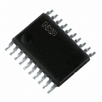
PCA9665PW,118 NXP Semiconductors, PCA9665PW,118 Datasheet - Page 31

PCA9665PW,118
Manufacturer Part Number
PCA9665PW,118
Description
IC CNTRLR PARALLEL/I2C 20TSSOP
Manufacturer
NXP Semiconductors
Datasheet
1.PCA9665D118.pdf
(90 pages)
Specifications of PCA9665PW,118
Package / Case
20-TSSOP
Controller Type
I²C Bus Controller
Interface
I²C
Voltage - Supply
2.3 V ~ 3.6 V
Current - Supply
100µA
Operating Temperature
-40°C ~ 85°C
Mounting Type
Surface Mount
Maximum Operating Temperature
+ 85 C
Minimum Operating Temperature
- 40 C
Mounting Style
SMD/SMT
Lead Free Status / RoHS Status
Lead free / RoHS Compliant
Lead Free Status / RoHS Status
Lead free / RoHS Compliant, Lead free / RoHS Compliant
Other names
568-4070-2
935279244118
PCA9665PW-T
PCA9665PW-T
935279244118
PCA9665PW-T
PCA9665PW-T
NXP Semiconductors
PCA9665_3
Product data sheet
8.4.1 Master Transmitter Buffered mode
8.4 Buffered mode
In the Master Transmitter Buffered mode, a number of data bytes are transmitted to a
slave receiver several bytes at a time (see
Buffered mode can be entered, I2CCON must be initialized as shown in
Table 33.
Table 34.
ENSIO must be set to logic 1 to enable the PCA9665. If the AA bit is reset, the PCA9665
will not acknowledge its own slave address in the event of another device becoming
master of the bus (in other words, if AA is reset, the PCA9665 cannot enter a slave mode).
STA, STO, and SI must be reset. Once ENSIO has been set to logic 1, it takes about
550 s for the oscillator to start up.
The Master Transmitter Buffered mode may now be entered by setting the STA bit. The
I
as the bus becomes free. When a START condition is transmitted, the Serial Interrupt flag
(SI) is set, the Interrupt line (INT) goes LOW and the status code in the status register
(I2CSTA) will be 08h. This status code must be used to vector to an interrupt service
routine that loads I2CDAT with the slave address and the data direction bit (SLA+W)
followed by the number of data bytes to be sent. The byte count register (I2CCOUNT) has
been previously programmed with the number of bytes that need to be sent in a single
sequence (BC[6:0]) as shown in
modes and can be programmed to either logic 0 or logic 1. The total number of bytes
loaded in I2CDAT (slave address with direction bit plus data bytes) must be equal to the
value programmed in I2CCOUNT. A write to I2CCON resets the SI bit, clears the Interrupt
(INT goes HIGH) and allows the serial transfer to continue.
When the slave address with the direction bit and part of or all the following bytes have
been transmitted, the Serial Interrupt flag (SI) is set again, the Interrupt line (INT) goes
LOW again and I2CSTA is loaded with the following possible codes:
Bit
Symbol
Value
Bit
Symbol
Value
2
C-bus state machine will first test the I
•
•
•
18h if an acknowledgment bit (ACK) has been received for the slave address with
direction bit (happens only if I2CCOUNT = 1; no data bytes have been sent).
20h if a no acknowledgment bit (NACK) has been received for the slave address with
direction bit (no data bytes have been sent).
28h if the slave address with direction bit and all the data bytes have been transmitted
and an acknowledgement bit has been received for each of them (number of bytes
sent is equal to value in I2CCOUNT).
I2CCON initialization (Buffered mode)
I2CCOUNT programming
AA
LB
X
X
7
7
Rev. 03 — 12 August 2008
ENSIO
BC6
number of bytes received in a single sequence (1 byte to 68 bytes)
6
1
6
Table
BC5
STA
5
0
5
34. LB bit is only used for the Receiver Buffered
2
C-bus and generate a START condition as soon
Figure
STO
BC4
4
0
4
Fm+ parallel bus to I
11). Before the Master Transmitter
BC3
SI
3
0
3
reserved reserved
BC2
X
2
2
PCA9665
© NXP B.V. 2008. All rights reserved.
2
C-bus controller
Table
BC1
X
1
1
33.
MODE
BC0
31 of 90
0
1
0


