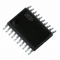
PCA9665PW,118 NXP Semiconductors, PCA9665PW,118 Datasheet - Page 73

PCA9665PW,118
Manufacturer Part Number
PCA9665PW,118
Description
IC CNTRLR PARALLEL/I2C 20TSSOP
Manufacturer
NXP Semiconductors
Datasheet
1.PCA9665D118.pdf
(90 pages)
Specifications of PCA9665PW,118
Package / Case
20-TSSOP
Controller Type
I²C Bus Controller
Interface
I²C
Voltage - Supply
2.3 V ~ 3.6 V
Current - Supply
100µA
Operating Temperature
-40°C ~ 85°C
Mounting Type
Surface Mount
Maximum Operating Temperature
+ 85 C
Minimum Operating Temperature
- 40 C
Mounting Style
SMD/SMT
Lead Free Status / RoHS Status
Lead free / RoHS Compliant
Lead Free Status / RoHS Status
Lead free / RoHS Compliant, Lead free / RoHS Compliant
Other names
568-4070-2
935279244118
PCA9665PW-T
PCA9665PW-T
935279244118
PCA9665PW-T
PCA9665PW-T
NXP Semiconductors
Table 50.
V
[1]
[2]
[3]
[4]
[5]
[6]
PCA9665_3
Product data sheet
Symbol
Initialization timing
t
Serial interface initialization timing
t
RESET timing (see
t
t
t
INT timing (see
t
t
Bus timing (see
t
t
t
t
t
t
t
t
t
t
t
t
init(po)
init(sintf)
w(rst)
rst
rec(rst)
as(int)
das(int)
su(A)
h(A)
su(CE_N)
h(CE_N)
w(RDL)
w(WRL)
d(DV)
d(QZ)
su(Q)
h(Q)
w(RDH)
w(WRH)
CC
= 2.5 V
Parameters are valid over specified temperature and voltage range.
All voltage measurements are referenced to ground (GND). For testing, all inputs swing between 0 V and 3.0 V with a transition time of
5 ns maximum. All time measurements are referenced at input voltages of 1.5 V and output voltages shown in
Test conditions for outputs: C
Test conditions for open-drain outputs: C
Initialization time for the serial interface after ENSIO bit goes HIGH in a write operation to the control register.
Resetting the device while actively communicating on the bus may cause glitches or an errant STOP condition.
Upon reset, the full delay will be the sum of t
Dynamic characteristics (2.5 volt)
Parameter
power-on initialization time
serial interface initialization time
reset pulse width
reset time
reset recovery time
interrupt assert time
interrupt de-assert time
address set-up time
address hold time
CE set-up time
CE hold time
RD LOW pulse width
WR LOW pulse width
data valid delay time
data output float delay time
data output set-up time
data output hold time
RD HIGH pulse width
WR HIGH pulse width
0.2 V; T
Figure
Figure 39
Figure
amb
38)
= 40 C to +85 C; unless otherwise specified. (See
37)
and
L
= 50 pF; R
Figure
L
41)
L
= 50 pF; R
= 500 , except open-drain outputs.
rst
[4]
and the RC time constant of the SDA and SCL bus.
[1][2][3]
Rev. 03 — 12 August 2008
Conditions
from ENSIO bit HIGH
to RD, WR LOW
from RD, WR LOW
to RD, WR LOW
from RD, WR LOW
after RD and CE LOW
after RD or CE HIGH
before WR or CE HIGH (write cycle)
after WR HIGH
L
= 1 k pull-up to V
DD
.
Table 49 on page 72
Fm+ parallel bus to I
[5][6]
Min
-
-
10
250
0
-
-
0
13
0
0
20
20
-
-
12
0
18
18
for 3.3 V)
Figure 39
PCA9665
Typ
-
-
-
-
-
-
-
-
-
-
-
-
-
-
-
-
-
-
-
© NXP B.V. 2008. All rights reserved.
2
C-bus controller
Max
550
550
-
-
-
550
20
-
-
-
-
-
-
22
17
-
-
-
-
and
Figure
73 of 90
Unit
ns
ns
ns
ns
ns
ns
ns
ns
ns
ns
ns
ns
ns
ns
ns
ns
ns
s
s
41.


