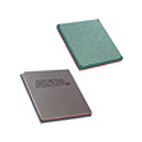
EP2S130F1020I5N Altera, EP2S130F1020I5N Datasheet - Page 118

EP2S130F1020I5N
Manufacturer Part Number
EP2S130F1020I5N
Description
Manufacturer
Altera
Datasheet
1.EP2S130F1020I5N.pdf
(238 pages)
Specifications of EP2S130F1020I5N
Family Name
Stratix II
Number Of Logic Blocks/elements
132540
# I/os (max)
742
Frequency (max)
609.76MHz
Process Technology
90nm (CMOS)
Operating Supply Voltage (typ)
1.2V
Logic Cells
132540
Ram Bits
6747840
Operating Supply Voltage (min)
1.15V
Operating Supply Voltage (max)
1.25V
Operating Temp Range
-40C to 100C
Operating Temperature Classification
Industrial
Mounting
Surface Mount
Pin Count
1020
Package Type
FC-FBGA
Lead Free Status / Rohs Status
Compliant
Available stocks
Company
Part Number
Manufacturer
Quantity
Price
Company:
Part Number:
EP2S130F1020I5N
Manufacturer:
ALTERA
Quantity:
215
Part Number:
EP2S130F1020I5N
Manufacturer:
ALTERA/阿尔特拉
Quantity:
20 000
- Current page: 118 of 238
- Download datasheet (3Mb)
SignalTap II Embedded Logic Analyzer
SignalTap II
Embedded Logic
Analyzer
Configuration
3–4
Stratix II Device Handbook, Volume 1
f
For more information on JTAG, see the following documents:
■
■
Stratix II devices feature the SignalTap II embedded logic analyzer, which
monitors design operation over a period of time through the IEEE
Std. 1149.1 (JTAG) circuitry. You can analyze internal logic at speed
without bringing internal signals to the I/O pins. This feature is
particularly important for advanced packages, such as FineLine BGA
packages, because it can be difficult to add a connection to a pin during
the debugging process after a board is designed and manufactured.
The logic, circuitry, and interconnects in the Stratix II architecture are
configured with CMOS SRAM elements. Altera
reconfigurable and every device is tested with a high coverage
production test program so you do not have to perform fault testing and
can instead focus on simulation and design verification.
Stratix II devices are configured at system power-up with data stored in
an Altera configuration device or provided by an external controller (e.g.,
a MAX
using the fast passive parallel (FPP), active serial (AS), passive serial (PS),
passive parallel asynchronous (PPA), and JTAG configuration schemes.
The Stratix II device’s optimized interface allows microprocessors to
configure it serially or in parallel, and synchronously or asynchronously.
The interface also enables microprocessors to treat Stratix II devices as
memory and configure them by writing to a virtual memory location,
making reconfiguration easy.
In addition to the number of configuration methods supported, Stratix II
devices also offer the design security, decompression, and remote system
upgrade features. The design security feature, using configuration
bitstream encryption and AES technology, provides a mechanism to
protect your designs. The decompression feature allows Stratix II FPGAs
to receive a compressed configuration bitstream and decompress this
data in real-time, reducing storage requirements and configuration time.
The remote system upgrade feature allows real-time system upgrades
from remote locations of your Stratix II designs. For more information,
see
“Configuration Schemes” on page
The IEEE Std. 1149.1 (JTAG) Boundary-Scan Testing for Stratix II &
Stratix II GX Devices chapter of the Stratix II Device Handbook,
Volume 2 or the Stratix II GX Device Handbook, Volume 2
Jam Programming & Test Language Specification
®
II device or microprocessor). Stratix II devices can be configured
3–7.
®
FPGA devices are
Altera Corporation
May 2007
®
Related parts for EP2S130F1020I5N
Image
Part Number
Description
Manufacturer
Datasheet
Request
R

Part Number:
Description:
CYCLONE II STARTER KIT EP2C20N
Manufacturer:
Altera
Datasheet:

Part Number:
Description:
CPLD, EP610 Family, ECMOS Process, 300 Gates, 16 Macro Cells, 16 Reg., 16 User I/Os, 5V Supply, 35 Speed Grade, 24DIP
Manufacturer:
Altera Corporation
Datasheet:

Part Number:
Description:
CPLD, EP610 Family, ECMOS Process, 300 Gates, 16 Macro Cells, 16 Reg., 16 User I/Os, 5V Supply, 15 Speed Grade, 24DIP
Manufacturer:
Altera Corporation
Datasheet:

Part Number:
Description:
Manufacturer:
Altera Corporation
Datasheet:

Part Number:
Description:
CPLD, EP610 Family, ECMOS Process, 300 Gates, 16 Macro Cells, 16 Reg., 16 User I/Os, 5V Supply, 30 Speed Grade, 24DIP
Manufacturer:
Altera Corporation
Datasheet:

Part Number:
Description:
High-performance, low-power erasable programmable logic devices with 8 macrocells, 10ns
Manufacturer:
Altera Corporation
Datasheet:

Part Number:
Description:
High-performance, low-power erasable programmable logic devices with 8 macrocells, 7ns
Manufacturer:
Altera Corporation
Datasheet:

Part Number:
Description:
Classic EPLD
Manufacturer:
Altera Corporation
Datasheet:

Part Number:
Description:
High-performance, low-power erasable programmable logic devices with 8 macrocells, 10ns
Manufacturer:
Altera Corporation
Datasheet:

Part Number:
Description:
Manufacturer:
Altera Corporation
Datasheet:

Part Number:
Description:
Manufacturer:
Altera Corporation
Datasheet:

Part Number:
Description:
Manufacturer:
Altera Corporation
Datasheet:

Part Number:
Description:
CPLD, EP610 Family, ECMOS Process, 300 Gates, 16 Macro Cells, 16 Reg., 16 User I/Os, 5V Supply, 25 Speed Grade, 24DIP
Manufacturer:
Altera Corporation
Datasheet:


