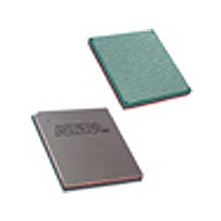
EP2S130F1020I5N Altera, EP2S130F1020I5N Datasheet - Page 97

EP2S130F1020I5N
Manufacturer Part Number
EP2S130F1020I5N
Description
Manufacturer
Altera
Datasheet
1.EP2S130F1020I5N.pdf
(238 pages)
Specifications of EP2S130F1020I5N
Family Name
Stratix II
Number Of Logic Blocks/elements
132540
# I/os (max)
742
Frequency (max)
609.76MHz
Process Technology
90nm (CMOS)
Operating Supply Voltage (typ)
1.2V
Logic Cells
132540
Ram Bits
6747840
Operating Supply Voltage (min)
1.15V
Operating Supply Voltage (max)
1.25V
Operating Temp Range
-40C to 100C
Operating Temperature Classification
Industrial
Mounting
Surface Mount
Pin Count
1020
Package Type
FC-FBGA
Lead Free Status / Rohs Status
Compliant
Available stocks
Company
Part Number
Manufacturer
Quantity
Price
Company:
Part Number:
EP2S130F1020I5N
Manufacturer:
ALTERA
Quantity:
215
Part Number:
EP2S130F1020I5N
Manufacturer:
ALTERA/阿尔特拉
Quantity:
20 000
- Current page: 97 of 238
- Download datasheet (3Mb)
Altera Corporation
May 2007
Each I/O bank has its own VCCIO pins. A single device can support
1.5-, 1.8-, 2.5-, and 3.3-V interfaces; each bank can support a different
V
support the voltage-referenced standards (such as SSTL-2). The PLL
banks utilize the adjacent VREF group when voltage-referenced
standards are implemented. For example, if an SSTL input is
implemented in PLL bank 10, the voltage level at VREFB7 is the reference
voltage level for the SSTL input.
I/O pins that reside in PLL banks 9 through 12 are powered by the
VCC_PLL<5, 6, 11, or 12>_OUT pins, respectively. The EP2S60F484,
EP2S60F780, EP2S90H484, EP2S90F780, and EP2S130F780 devices do not
support PLLs 11 and 12. Therefore, any I/O pins that reside in bank 11 are
powered by the VCCIO3 pin, and any I/O pins that reside in bank 12 are
powered by the VCCIO8 pin.
Each I/O bank can support multiple standards with the same V
input and output pins. Each bank can support one V
example, when V
3.3-V PCI for inputs and outputs.
On-Chip Termination
Stratix II devices provide differential (for the LVDS or HyperTransport
technology I/O standard), series, and parallel on-chip termination to
reduce reflections and maintain signal integrity. On-chip termination
simplifies board design by minimizing the number of external
termination resistors required. Termination can be placed inside the
package, eliminating small stubs that can still lead to reflections.
Stratix II devices provide four types of termination:
■
■
■
■
CCIO
Differential termination (R
Series termination (R
Series termination (R
Parallel termination (R
level independently. Each bank also has dedicated VREF pins to
CCIO
is 3.3 V, a bank can support LVTTL, LVCMOS, and
S
S
) without calibration
) with calibration
T
) with calibration
D
)
Stratix II Device Handbook, Volume 1
REF
Stratix II Architecture
voltage level. For
CCIO
2–89
for
Related parts for EP2S130F1020I5N
Image
Part Number
Description
Manufacturer
Datasheet
Request
R

Part Number:
Description:
CYCLONE II STARTER KIT EP2C20N
Manufacturer:
Altera
Datasheet:

Part Number:
Description:
CPLD, EP610 Family, ECMOS Process, 300 Gates, 16 Macro Cells, 16 Reg., 16 User I/Os, 5V Supply, 35 Speed Grade, 24DIP
Manufacturer:
Altera Corporation
Datasheet:

Part Number:
Description:
CPLD, EP610 Family, ECMOS Process, 300 Gates, 16 Macro Cells, 16 Reg., 16 User I/Os, 5V Supply, 15 Speed Grade, 24DIP
Manufacturer:
Altera Corporation
Datasheet:

Part Number:
Description:
Manufacturer:
Altera Corporation
Datasheet:

Part Number:
Description:
CPLD, EP610 Family, ECMOS Process, 300 Gates, 16 Macro Cells, 16 Reg., 16 User I/Os, 5V Supply, 30 Speed Grade, 24DIP
Manufacturer:
Altera Corporation
Datasheet:

Part Number:
Description:
High-performance, low-power erasable programmable logic devices with 8 macrocells, 10ns
Manufacturer:
Altera Corporation
Datasheet:

Part Number:
Description:
High-performance, low-power erasable programmable logic devices with 8 macrocells, 7ns
Manufacturer:
Altera Corporation
Datasheet:

Part Number:
Description:
Classic EPLD
Manufacturer:
Altera Corporation
Datasheet:

Part Number:
Description:
High-performance, low-power erasable programmable logic devices with 8 macrocells, 10ns
Manufacturer:
Altera Corporation
Datasheet:

Part Number:
Description:
Manufacturer:
Altera Corporation
Datasheet:

Part Number:
Description:
Manufacturer:
Altera Corporation
Datasheet:

Part Number:
Description:
Manufacturer:
Altera Corporation
Datasheet:

Part Number:
Description:
CPLD, EP610 Family, ECMOS Process, 300 Gates, 16 Macro Cells, 16 Reg., 16 User I/Os, 5V Supply, 25 Speed Grade, 24DIP
Manufacturer:
Altera Corporation
Datasheet:


