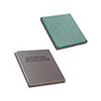
EP2S130F1020I5N Altera, EP2S130F1020I5N Datasheet - Page 78

EP2S130F1020I5N
Manufacturer Part Number
EP2S130F1020I5N
Description
Manufacturer
Altera
Datasheet
1.EP2S130F1020I5N.pdf
(238 pages)
Specifications of EP2S130F1020I5N
Family Name
Stratix II
Number Of Logic Blocks/elements
132540
# I/os (max)
742
Frequency (max)
609.76MHz
Process Technology
90nm (CMOS)
Operating Supply Voltage (typ)
1.2V
Logic Cells
132540
Ram Bits
6747840
Operating Supply Voltage (min)
1.15V
Operating Supply Voltage (max)
1.25V
Operating Temp Range
-40C to 100C
Operating Temperature Classification
Industrial
Mounting
Surface Mount
Pin Count
1020
Package Type
FC-FBGA
Lead Free Status / Rohs Status
Compliant
Available stocks
Company
Part Number
Manufacturer
Quantity
Price
Company:
Part Number:
EP2S130F1020I5N
Manufacturer:
ALTERA
Quantity:
215
Part Number:
EP2S130F1020I5N
Manufacturer:
ALTERA/阿尔特拉
Quantity:
20 000
- Current page: 78 of 238
- Download datasheet (3Mb)
I/O Structure
2–70
Stratix II Device Handbook, Volume 1
■
■
■
■
■
■
■
■
The IOE in Stratix II devices contains a bidirectional I/O buffer, six
registers, and a latch for a complete embedded bidirectional single data
rate or DDR transfer.
IOE contains two input registers (plus a latch), two output registers, and
two output enable registers. The design can use both input registers and
the latch to capture DDR input and both output registers to drive DDR
outputs. Additionally, the design can use the output enable (OE) register
for fast clock-to-output enable timing. The negative edge-clocked OE
register is used for DDR SDRAM interfacing. The Quartus II software
automatically duplicates a single OE register that controls multiple
output or bidirectional pins.
Output drive strength control
Tri-state buffers
Bus-hold circuitry
Programmable pull-up resistors
Programmable input and output delays
Open-drain outputs
DQ and DQS I/O pins
Double data rate (DDR) registers
Figure 2–46
shows the Stratix II IOE structure. The
Altera Corporation
May 2007
Related parts for EP2S130F1020I5N
Image
Part Number
Description
Manufacturer
Datasheet
Request
R

Part Number:
Description:
CYCLONE II STARTER KIT EP2C20N
Manufacturer:
Altera
Datasheet:

Part Number:
Description:
CPLD, EP610 Family, ECMOS Process, 300 Gates, 16 Macro Cells, 16 Reg., 16 User I/Os, 5V Supply, 35 Speed Grade, 24DIP
Manufacturer:
Altera Corporation
Datasheet:

Part Number:
Description:
CPLD, EP610 Family, ECMOS Process, 300 Gates, 16 Macro Cells, 16 Reg., 16 User I/Os, 5V Supply, 15 Speed Grade, 24DIP
Manufacturer:
Altera Corporation
Datasheet:

Part Number:
Description:
Manufacturer:
Altera Corporation
Datasheet:

Part Number:
Description:
CPLD, EP610 Family, ECMOS Process, 300 Gates, 16 Macro Cells, 16 Reg., 16 User I/Os, 5V Supply, 30 Speed Grade, 24DIP
Manufacturer:
Altera Corporation
Datasheet:

Part Number:
Description:
High-performance, low-power erasable programmable logic devices with 8 macrocells, 10ns
Manufacturer:
Altera Corporation
Datasheet:

Part Number:
Description:
High-performance, low-power erasable programmable logic devices with 8 macrocells, 7ns
Manufacturer:
Altera Corporation
Datasheet:

Part Number:
Description:
Classic EPLD
Manufacturer:
Altera Corporation
Datasheet:

Part Number:
Description:
High-performance, low-power erasable programmable logic devices with 8 macrocells, 10ns
Manufacturer:
Altera Corporation
Datasheet:

Part Number:
Description:
Manufacturer:
Altera Corporation
Datasheet:

Part Number:
Description:
Manufacturer:
Altera Corporation
Datasheet:

Part Number:
Description:
Manufacturer:
Altera Corporation
Datasheet:

Part Number:
Description:
CPLD, EP610 Family, ECMOS Process, 300 Gates, 16 Macro Cells, 16 Reg., 16 User I/Os, 5V Supply, 25 Speed Grade, 24DIP
Manufacturer:
Altera Corporation
Datasheet:


