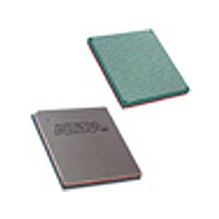
EP2S130F1020I5N Altera, EP2S130F1020I5N Datasheet - Page 213

EP2S130F1020I5N
Manufacturer Part Number
EP2S130F1020I5N
Description
Manufacturer
Altera
Datasheet
1.EP2S130F1020I5N.pdf
(238 pages)
Specifications of EP2S130F1020I5N
Family Name
Stratix II
Number Of Logic Blocks/elements
132540
# I/os (max)
742
Frequency (max)
609.76MHz
Process Technology
90nm (CMOS)
Operating Supply Voltage (typ)
1.2V
Logic Cells
132540
Ram Bits
6747840
Operating Supply Voltage (min)
1.15V
Operating Supply Voltage (max)
1.25V
Operating Temp Range
-40C to 100C
Operating Temperature Classification
Industrial
Mounting
Surface Mount
Pin Count
1020
Package Type
FC-FBGA
Lead Free Status / Rohs Status
Compliant
Available stocks
Company
Part Number
Manufacturer
Quantity
Price
Company:
Part Number:
EP2S130F1020I5N
Manufacturer:
ALTERA
Quantity:
215
Part Number:
EP2S130F1020I5N
Manufacturer:
ALTERA/阿尔特拉
Quantity:
20 000
- Current page: 213 of 238
- Download datasheet (3Mb)
Duty Cycle
Distortion
Altera Corporation
April 2011
Notes to
(1)
(2)
(3)
(4)
3.3-V LVTTL
2.5-V LVTTL
1.8-V LVTTL
3.3-V LVCMOS
1.5-V LVCMOS
SSTL-2 Class I
SSTL-2 Class II
SSTL-18 Class I
SSTL-18 Class II
1.2-V HSTL
Table 5–79. Maximum Output Clock Toggle Rate Derating Factors (Part 5 of 5)
I/O Standard
For LVDS and HyperTransport technology output on row I/O pins, the toggle rate derating factors apply to loads
larger than 5 pF. In the derating calculation, subtract 5 pF from the intended load value in pF for the correct result.
For a load less than or equal to 5 pF, refer to
1.2-V HSTL is only supported on column I/O pins in I/O banks 4,7, and 8.
Differential HSTL and SSTL is only supported on column clock and DQS outputs.
LVPECL is only supported on column clock outputs.
Table
(2)
5–79:
Strength
Drive
OCT
50 Ω
OCT
50 Ω
OCT
50 Ω
OCT
50 Ω
OCT
50 Ω
OCT
50 Ω
OCT
25 Ω
OCT
50 Ω
OCT
25 Ω
OCT
50 Ω
Duty cycle distortion (DCD) describes how much the falling edge of a
clock is off from its ideal position. The ideal position is when both the
clock high time (CLKH) and the clock low time (CLKL) equal half of the
clock period (T), as shown in
non-ideal falling edge from the ideal falling edge, such as D1 for the
falling edge A and D2 for the falling edge B
DCD for a clock is the larger value of D1 and D2.
133
207
151
300
157
121
100
56
61
95
-3
Column I/O Pins
Maximum Output Clock Toggle Rate Derating Factors (ps/pF)
152
274
165
316
171
134
101
123
110
-4
-
Table 5–78
152
274
165
316
171
134
101
123
110
-5
-
for output toggle rates.
133
207
151
300
157
121
100
56
-3
-
-
Figure
Row I/O Pins
152
274
165
316
171
134
101
123
-4
-
-
5–7. DCD is the deviation of the
Stratix II Device Handbook, Volume 1
DC & Switching Characteristics
152
274
165
316
171
134
101
123
-5
-
-
(Figure
Dedicated Clock Outputs
147
235
153
263
174
106
77
58
59
-3
-
5–7). The maximum
152
274
165
316
171
134
101
123
110
-4
-
152
274
165
316
171
134
101
123
110
95
-5
5–77
Related parts for EP2S130F1020I5N
Image
Part Number
Description
Manufacturer
Datasheet
Request
R

Part Number:
Description:
CYCLONE II STARTER KIT EP2C20N
Manufacturer:
Altera
Datasheet:

Part Number:
Description:
CPLD, EP610 Family, ECMOS Process, 300 Gates, 16 Macro Cells, 16 Reg., 16 User I/Os, 5V Supply, 35 Speed Grade, 24DIP
Manufacturer:
Altera Corporation
Datasheet:

Part Number:
Description:
CPLD, EP610 Family, ECMOS Process, 300 Gates, 16 Macro Cells, 16 Reg., 16 User I/Os, 5V Supply, 15 Speed Grade, 24DIP
Manufacturer:
Altera Corporation
Datasheet:

Part Number:
Description:
Manufacturer:
Altera Corporation
Datasheet:

Part Number:
Description:
CPLD, EP610 Family, ECMOS Process, 300 Gates, 16 Macro Cells, 16 Reg., 16 User I/Os, 5V Supply, 30 Speed Grade, 24DIP
Manufacturer:
Altera Corporation
Datasheet:

Part Number:
Description:
High-performance, low-power erasable programmable logic devices with 8 macrocells, 10ns
Manufacturer:
Altera Corporation
Datasheet:

Part Number:
Description:
High-performance, low-power erasable programmable logic devices with 8 macrocells, 7ns
Manufacturer:
Altera Corporation
Datasheet:

Part Number:
Description:
Classic EPLD
Manufacturer:
Altera Corporation
Datasheet:

Part Number:
Description:
High-performance, low-power erasable programmable logic devices with 8 macrocells, 10ns
Manufacturer:
Altera Corporation
Datasheet:

Part Number:
Description:
Manufacturer:
Altera Corporation
Datasheet:

Part Number:
Description:
Manufacturer:
Altera Corporation
Datasheet:

Part Number:
Description:
Manufacturer:
Altera Corporation
Datasheet:

Part Number:
Description:
CPLD, EP610 Family, ECMOS Process, 300 Gates, 16 Macro Cells, 16 Reg., 16 User I/Os, 5V Supply, 25 Speed Grade, 24DIP
Manufacturer:
Altera Corporation
Datasheet:


