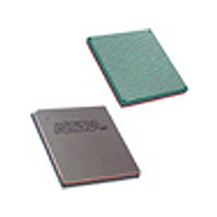
EP2S130F1020I5N Altera, EP2S130F1020I5N Datasheet - Page 139

EP2S130F1020I5N
Manufacturer Part Number
EP2S130F1020I5N
Description
Manufacturer
Altera
Datasheet
1.EP2S130F1020I5N.pdf
(238 pages)
Specifications of EP2S130F1020I5N
Family Name
Stratix II
Number Of Logic Blocks/elements
132540
# I/os (max)
742
Frequency (max)
609.76MHz
Process Technology
90nm (CMOS)
Operating Supply Voltage (typ)
1.2V
Logic Cells
132540
Ram Bits
6747840
Operating Supply Voltage (min)
1.15V
Operating Supply Voltage (max)
1.25V
Operating Temp Range
-40C to 100C
Operating Temperature Classification
Industrial
Mounting
Surface Mount
Pin Count
1020
Package Type
FC-FBGA
Lead Free Status / Rohs Status
Compliant
Available stocks
Company
Part Number
Manufacturer
Quantity
Price
Company:
Part Number:
EP2S130F1020I5N
Manufacturer:
ALTERA
Quantity:
215
Part Number:
EP2S130F1020I5N
Manufacturer:
ALTERA/阿尔特拉
Quantity:
20 000
- Current page: 139 of 238
- Download datasheet (3Mb)
Altera Corporation
April 2011
Notes to
(1)
(2)
(3)
(4)
(5)
(6)
(7)
T
I
I
I
I
Symbol
Symbol
I
OZ
C C I N T 0
CCPD0
Table 5–3. Stratix II Device Recommended Operating Conditions (Part 2 of 2)
Table 5–4. Stratix II Device DC Operating Conditions (Part 1 of 2)
J
Supply voltage specifications apply to voltage readings taken at the device pins, not at the power supply.
During transitions, the inputs may overshoot to the voltage shown in
The DC case is equivalent to 100% duty cycle. During transitions, the inputs may undershoot to –2.0 V for input
currents less than 100 mA and periods shorter than 20 ns.
Maximum V
V
time, your Stratix II device does not configure successfully. If your system does not allow for a V
of 100 ms or less, you must hold nCONFIG low until all power supplies are reliable.
All pins, including dedicated inputs, clock, I/O, and JTAG pins, may be driven before V
are powered.
V
For more information, refer to the
CCPD
C C I O
Table
Operating junction temperature
Input pin leakage current V
Tri-stated I/O pin
leakage current
V
(standby)
V
(standby)
must ramp-up from 0 V to 3.3 V within 100 μs to 100 ms. If V
maximum and minimum conditions for PCI and PCI-X are shown in parentheses.
CCINT
CCPD
5–3:
CC
supply current
Parameter
supply current
rise time is 100 ms, and V
Parameter
DC Electrical Characteristics
Table 5–4
Stratix II Military Temperature Range Support
V
V
load, no toggling
inputs
T
V
load, no toggling
inputs
T
V
O
J
J
I
I
I
CCPD
= V
= ground, no
= ground, no
= 25° C
= 25° C,
= V
shows the Stratix II device family DC electrical characteristics.
CC
CCIOmax
= 3.3V
CCIOmax
For commercial use
For industrial use
For military use
must rise monotonically from ground to V
Conditions
to 0 V
to 0 V
Conditions
(2)
EP2S15
EP2S30
EP2S60
EP2S90
EP2S130
EP2S180
EP2S15
EP2S30
EP2S60
EP2S90
EP2S130
EP2S180
(2)
(7)
C C P D
Table 5–2
Minimum Typical Maximum Unit
Stratix II Device Handbook, Volume 1
is not ramped up within this specified
Note (1)
–10
–10
DC & Switching Characteristics
technical brief.
based upon the input duty cycle.
Minimum
–40
–55
0
0.25
0.30
0.50
0.62
0.82
1.12
C C
2.2
2.7
3.6
4.3
5.4
6.8
Note (1)
CCINT
.
, V
CCPD
Maximum Unit
CCPD
100
125
(3)
(3)
(3)
(3)
(3)
(3)
(3)
(3)
(3)
(3)
(3)
(3)
10
10
85
ramp-up time
, and V
CCIO
mA
mA
mA
mA
mA
mA
μA
μA
A
A
A
A
A
A
°C
°C
°C
5–3
Related parts for EP2S130F1020I5N
Image
Part Number
Description
Manufacturer
Datasheet
Request
R

Part Number:
Description:
CYCLONE II STARTER KIT EP2C20N
Manufacturer:
Altera
Datasheet:

Part Number:
Description:
CPLD, EP610 Family, ECMOS Process, 300 Gates, 16 Macro Cells, 16 Reg., 16 User I/Os, 5V Supply, 35 Speed Grade, 24DIP
Manufacturer:
Altera Corporation
Datasheet:

Part Number:
Description:
CPLD, EP610 Family, ECMOS Process, 300 Gates, 16 Macro Cells, 16 Reg., 16 User I/Os, 5V Supply, 15 Speed Grade, 24DIP
Manufacturer:
Altera Corporation
Datasheet:

Part Number:
Description:
Manufacturer:
Altera Corporation
Datasheet:

Part Number:
Description:
CPLD, EP610 Family, ECMOS Process, 300 Gates, 16 Macro Cells, 16 Reg., 16 User I/Os, 5V Supply, 30 Speed Grade, 24DIP
Manufacturer:
Altera Corporation
Datasheet:

Part Number:
Description:
High-performance, low-power erasable programmable logic devices with 8 macrocells, 10ns
Manufacturer:
Altera Corporation
Datasheet:

Part Number:
Description:
High-performance, low-power erasable programmable logic devices with 8 macrocells, 7ns
Manufacturer:
Altera Corporation
Datasheet:

Part Number:
Description:
Classic EPLD
Manufacturer:
Altera Corporation
Datasheet:

Part Number:
Description:
High-performance, low-power erasable programmable logic devices with 8 macrocells, 10ns
Manufacturer:
Altera Corporation
Datasheet:

Part Number:
Description:
Manufacturer:
Altera Corporation
Datasheet:

Part Number:
Description:
Manufacturer:
Altera Corporation
Datasheet:

Part Number:
Description:
Manufacturer:
Altera Corporation
Datasheet:

Part Number:
Description:
CPLD, EP610 Family, ECMOS Process, 300 Gates, 16 Macro Cells, 16 Reg., 16 User I/Os, 5V Supply, 25 Speed Grade, 24DIP
Manufacturer:
Altera Corporation
Datasheet:


