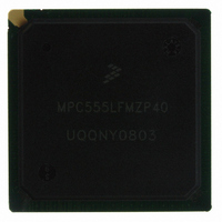
MPC555LFMZP40 Freescale Semiconductor, MPC555LFMZP40 Datasheet - Page 95

MPC555LFMZP40
Manufacturer Part Number
MPC555LFMZP40
Description
IC MCU 32BIT 40MHZ 272-BGA
Manufacturer
Freescale Semiconductor
Series
MPC5xxr
Datasheets
1.MPC555LFMZP40.pdf
(12 pages)
2.MPC555LFMZP40.pdf
(966 pages)
3.MPC555LFMZP40.pdf
(3 pages)
Specifications of MPC555LFMZP40
Core Processor
PowerPC
Core Size
32-Bit
Speed
40MHz
Connectivity
CAN, EBI/EMI, SCI, SPI, UART/USART
Peripherals
POR, PWM, WDT
Number Of I /o
101
Program Memory Size
448KB (448K x 8)
Program Memory Type
FLASH
Ram Size
26K x 8
Voltage - Supply (vcc/vdd)
2.5 V ~ 2.7 V
Data Converters
A/D 32x10b
Oscillator Type
External
Operating Temperature
-40°C ~ 125°C
Package / Case
272-PBGA
Controller Family/series
POWER 5xx
Ram Memory Size
26KB
Cpu Speed
63MIPS
Embedded Interface Type
QSPI, SCI, TouCAN
Operating Temperature Range
-40°C To +125°C
No. Of Pins
272
Rohs Compliant
No
Processor Series
MPC5xx
Core
PowerPC
Data Bus Width
32 bit
Data Ram Size
26 KB
Interface Type
CAN, QSPI, SCI
Maximum Clock Frequency
40 MHz
Number Of Programmable I/os
101
Operating Supply Voltage
3.3 V to 5 V
Maximum Operating Temperature
+ 125 C
Mounting Style
SMD/SMT
Development Tools By Supplier
MPC555CMEE
Minimum Operating Temperature
- 85 C
On-chip Adc
10 bit, 32 Channel
Cpu Family
MPC55xx
Device Core
PowerPC
Device Core Size
32b
Frequency (max)
40MHz
Total Internal Ram Size
32KB
# I/os (max)
101
Operating Supply Voltage (typ)
5V
Instruction Set Architecture
RISC
Operating Temp Range
-40C to 85C
Operating Temperature Classification
Industrial
Mounting
Surface Mount
Pin Count
272
Package Type
BGA
For Use With
MPC555CMEE - KIT EVAL FOR MPC555
Lead Free Status / RoHS Status
Contains lead / RoHS non-compliant
Eeprom Size
-
Lead Free Status / Rohs Status
No
Available stocks
Company
Part Number
Manufacturer
Quantity
Price
Company:
Part Number:
MPC555LFMZP40
Manufacturer:
MOTOLOLA
Quantity:
853
Company:
Part Number:
MPC555LFMZP40
Manufacturer:
Freescale Semiconductor
Quantity:
10 000
Company:
Part Number:
MPC555LFMZP40R2
Manufacturer:
Freescale Semiconductor
Quantity:
10 000
- Current page: 95 of 966
- Download datasheet (15Mb)
2.5 Pad Types
2.5.1 Pad Interface Signals
MPC555
USER’S MANUAL
NOTES:
There are different pad types based on functional characteristics. Even pads with the
same functionality may be different due to different electrical characteristics. All 5-V
inputs have hysteresis. There is no synchronization in the pads; it is all in the modules.
The pad interface consists of an internal interface and an external interface. The ex-
ternal interface is to the pin. The internal interface is the set of signals that interface
the pad to the chip’s internal logic. The following internal interface signals are used:
1. During reset, the output enable to the pad driver is negated and the PU3/PU5 is active. After reset is negated,
2. Pull-up/pull-down is active when pin is defined as an input and/or during reset; therefore, output enable is
3. These pins are powered by KAPWR (Keep-Alive Power Supply).
4. This pin is an active negate signal and may need an external pull-up resister.
VDDSRAM
KAPWR
VDDSYN
VSSSYN
the output enable is continuously enabled and the PU3 is disabled. The driver is responsible for driving a
valid state on the pin.
negated. This also means that external pull-up/pull-down is not required unless specified.
• Data – The line driven from an internal module of the chip to the pad. For bi-di-
• 3-V / 5-V select – Selects a 3-V or 5-V driver, for pads that support both. This sig-
• Output enable (OE) – Enables the output driver. For 3-V / 5-V pads, the appropri-
• Input enable – Enables the receiver. For 3-V / 5-V pads, the appropriate receiver
VDDH
VDDF
EPEE
VSSF
VDDL
VDDI
VSSI
VPP
VSS
/
rectional pins, the internal interface may be a single line for both input and output
or two separate paths for input and output. The descriptions of individual pad
types specify which.
nal is driven from the USIU.
ate driver is enabled based on the pin functionality selected.
is enabled based on the pin functionality selected.
Pin
MPC556
3
Function
VDDSRAM
Freescale Semiconductor, Inc.
VDDSYN
VSSSYN
KAPWR
Table 2-4 Pin Reset State (Continued)
VDDSI
VDDH
EPEE
VDDF
VDDL
VSSF
VSSI
VPP
VSS
For More Information On This Product,
Go to: www.freescale.com
SIGNAL DESCRIPTIONS
Rev. 15 October 2000
Global Power Supplies
Port
I
I
I
I
I
I
I
I
I
I
I
I
I
CMF
Voltage
3 V
5 V
3 V
3 V
3 V
5 V
3 V
3 V
3 V
3 V
3 V
3 V
—
PD
—
—
—
Reset State
—
—
—
—
—
—
—
—
—
MOTOROLA
2-37
Related parts for MPC555LFMZP40
Image
Part Number
Description
Manufacturer
Datasheet
Request
R
Part Number:
Description:
Manufacturer:
Freescale Semiconductor, Inc
Datasheet:
Part Number:
Description:
Manufacturer:
Freescale Semiconductor, Inc
Datasheet:
Part Number:
Description:
Manufacturer:
Freescale Semiconductor, Inc
Datasheet:
Part Number:
Description:
Manufacturer:
Freescale Semiconductor, Inc
Datasheet:
Part Number:
Description:
Manufacturer:
Freescale Semiconductor, Inc
Datasheet:
Part Number:
Description:
Manufacturer:
Freescale Semiconductor, Inc
Datasheet:
Part Number:
Description:
Manufacturer:
Freescale Semiconductor, Inc
Datasheet:
Part Number:
Description:
Manufacturer:
Freescale Semiconductor, Inc
Datasheet:
Part Number:
Description:
Manufacturer:
Freescale Semiconductor, Inc
Datasheet:
Part Number:
Description:
Manufacturer:
Freescale Semiconductor, Inc
Datasheet:
Part Number:
Description:
Manufacturer:
Freescale Semiconductor, Inc
Datasheet:
Part Number:
Description:
Manufacturer:
Freescale Semiconductor, Inc
Datasheet:
Part Number:
Description:
Manufacturer:
Freescale Semiconductor, Inc
Datasheet:
Part Number:
Description:
Manufacturer:
Freescale Semiconductor, Inc
Datasheet:
Part Number:
Description:
Manufacturer:
Freescale Semiconductor, Inc
Datasheet:


