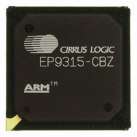
EP9315-CBZ Cirrus Logic Inc, EP9315-CBZ Datasheet - Page 43

EP9315-CBZ
Manufacturer Part Number
EP9315-CBZ
Description
IC ARM9 SOC ENH UNIV 352PBGA
Manufacturer
Cirrus Logic Inc
Series
EP9r
Specifications of EP9315-CBZ
Core Size
16/32-Bit
Core Processor
ARM9
Speed
200MHz
Connectivity
EBI/EMI, EIDE, Ethernet, I²C, IrDA, Keypad/Touchscreen, PCMCIA, SPI, UART/USART, USB
Peripherals
AC'97, DMA, I²:S, LCD, LED, MaverickKey, POR, PWM, WDT
Number Of I /o
16
Program Memory Type
ROMless
Ram Size
32K x 8
Voltage - Supply (vcc/vdd)
1.65 V ~ 3.6 V
Data Converters
A/D 8x12b
Oscillator Type
External
Operating Temperature
0°C ~ 70°C
Package / Case
352-BGA
Controller Family/series
(ARM9)
No. Of I/o's
16
Cpu Speed
200MHz
No. Of Timers
5
Digital Ic Case Style
BGA
Supply Voltage Range
1.65V To 1.94V, 3V To 3.6V
Embedded Interface Type
SPI
Rohs Compliant
Yes
Processor Series
EP93xx
Core
ARM920T
Data Bus Width
32 bit
3rd Party Development Tools
MDK-ARM, RL-ARM, ULINK2
Development Tools By Supplier
EDB9315A-Z
Case
BGA
Dc
06+
Lead Free Status / RoHS Status
Lead free / RoHS Compliant
For Use With
598-1144 - KIT DEVELOPMENT EP9315 ARM9
Eeprom Size
-
Program Memory Size
-
Lead Free Status / Rohs Status
Details
Other names
598-1139
Available stocks
Company
Part Number
Manufacturer
Quantity
Price
Part Number:
EP9315-CBZ
Manufacturer:
CIRRUS
Quantity:
20 000
- Current page: 43 of 824
- Download datasheet (13Mb)
DS785UM1
2.2.3.2.3
2.2.3.3.1
2.2.3.3 Cache and Write Buffer
Enabling the MMU allows system memory control, but is also required if the Data Cache and
the Write Buffer are to be used. Features are enabled for specific memory regions, as defined
in the system page table. MMU enablement is done via CP15 register 1. The procedure is as
follows:
Cache configuration is 64-way set associative. There is a 16 kbyte instruction cache and a 16
kbyte data cache. The caches have the following characteristics:
1. Program the Translation Table Base (TTB) and domain access control registers
2. Create level 1 and level 2 pages for the system, and enable the Data Cache and the
3. Enable the MMU via bit 0 of CP15 register 1.
• 8 words per line, with 1 valid bit and 2 dirty bits per line to allow half-line write-backs
• Write-through or write-back capability, selectable per memory region defined by the
• Pseudo random or round robin replacement algorithms for cache misses. This is
• Independent cache lock-down with granularity of 1/64th of total cache size or 256 bytes
• For compatibility with Windows CE and to reduce latency, physical addresses for data
• The Write Buffer has a depth of 16 data words. If enabled, writes are sent to the Write
• At reset, the Instruction Cache is disabled
• A write to bit 12 of CP15 register 1 will enable or disable the Instruction Cache. If the
• If the I-Cache is disabled, current contents are ignored. If re-enabled before a reset,
MMU
determined by the RR bit (bit 14) in CP15 register 1. On a cache miss (instruction or data
not in the respective cache), an 8-word line is fetched from memory and loaded into the
cache
for both instructions and data. Lock-down of the cache will prevent an eight-word cache
line fill into that region of the cache
cache entries are stored in the PA TAG RAM, which is used for cache line write-back
operations without need of the MMU. This prevents a possible TLB miss that would
degrade performance
Buffer directly from the Data Cache or from the CPU (in the event of a cache miss or if
the cache is not enabled).
Instruction Cache (I-Cache) is enabled without the MMU enabled, all accesses are
treated as cacheable
contents will be unchanged, but may not be coherent with eternal memory. If so,
contents must be flushed before re-enabling.
Write Buffer
MMU Enable
Instruction Cache Enable
Copyright 2007 Cirrus Logic
ARM920T Core and Advanced High-Speed Bus (AHB)
EP93xx User’s Guide
2-5
2
Related parts for EP9315-CBZ
Image
Part Number
Description
Manufacturer
Datasheet
Request
R

Part Number:
Description:
IC ARM920T MCU 200MHZ 352-PBGA
Manufacturer:
Cirrus Logic Inc
Datasheet:

Part Number:
Description:
32-Bit Microcontroller IC
Manufacturer:
Cirrus Logic Inc
Datasheet:

Part Number:
Description:
IC ARM920T MCU 200MHZ 352-PBGA
Manufacturer:
Cirrus Logic Inc
Datasheet:

Part Number:
Description:
MCU, MPU & DSP Development Tools Eval Bd Uni. ARM9 SOC Processor
Manufacturer:
Cirrus Logic Inc
Datasheet:

Part Number:
Description:
Development Kit
Manufacturer:
Cirrus Logic Inc
Datasheet:

Part Number:
Description:
Development Kit
Manufacturer:
Cirrus Logic Inc
Datasheet:

Part Number:
Description:
High-efficiency PFC + Fluorescent Lamp Driver Reference Design
Manufacturer:
Cirrus Logic Inc
Datasheet:

Part Number:
Description:
Development Kit
Manufacturer:
Cirrus Logic Inc
Datasheet:

Part Number:
Description:
Development Kit
Manufacturer:
Cirrus Logic Inc
Datasheet:

Part Number:
Description:
Development Kit
Manufacturer:
Cirrus Logic Inc
Datasheet:

Part Number:
Description:
Development Kit
Manufacturer:
Cirrus Logic Inc
Datasheet:

Part Number:
Description:
Development Kit
Manufacturer:
Cirrus Logic Inc
Datasheet:

Part Number:
Description:
Development Kit
Manufacturer:
Cirrus Logic Inc
Datasheet:

Part Number:
Description:
Ref Bd For Speakerbar MSA & DSP Products
Manufacturer:
Cirrus Logic Inc


