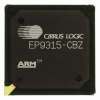
EP9315-CBZ Cirrus Logic Inc, EP9315-CBZ Datasheet - Page 714

EP9315-CBZ
Manufacturer Part Number
EP9315-CBZ
Description
IC ARM9 SOC ENH UNIV 352PBGA
Manufacturer
Cirrus Logic Inc
Series
EP9r
Specifications of EP9315-CBZ
Core Size
16/32-Bit
Core Processor
ARM9
Speed
200MHz
Connectivity
EBI/EMI, EIDE, Ethernet, I²C, IrDA, Keypad/Touchscreen, PCMCIA, SPI, UART/USART, USB
Peripherals
AC'97, DMA, I²:S, LCD, LED, MaverickKey, POR, PWM, WDT
Number Of I /o
16
Program Memory Type
ROMless
Ram Size
32K x 8
Voltage - Supply (vcc/vdd)
1.65 V ~ 3.6 V
Data Converters
A/D 8x12b
Oscillator Type
External
Operating Temperature
0°C ~ 70°C
Package / Case
352-BGA
Controller Family/series
(ARM9)
No. Of I/o's
16
Cpu Speed
200MHz
No. Of Timers
5
Digital Ic Case Style
BGA
Supply Voltage Range
1.65V To 1.94V, 3V To 3.6V
Embedded Interface Type
SPI
Rohs Compliant
Yes
Processor Series
EP93xx
Core
ARM920T
Data Bus Width
32 bit
3rd Party Development Tools
MDK-ARM, RL-ARM, ULINK2
Development Tools By Supplier
EDB9315A-Z
Case
BGA
Dc
06+
Lead Free Status / RoHS Status
Lead free / RoHS Compliant
For Use With
598-1144 - KIT DEVELOPMENT EP9315 ARM9
Eeprom Size
-
Program Memory Size
-
Lead Free Status / Rohs Status
Details
Other names
598-1139
Available stocks
Company
Part Number
Manufacturer
Quantity
Price
Part Number:
EP9315-CBZ
Manufacturer:
CIRRUS
Quantity:
20 000
- Current page: 714 of 824
- Download datasheet (13Mb)
23
23-2
Synchronous Serial Port
EP93xx User’s Guide
23.5.1 Enabling SSP Operation
23.3 SSP Functionality
23.4 SSP Pin Multiplex
23.5 Configuring the SSP
The SSP includes a programmable bit rate clock divider and prescaler to generate the serial
output clock SCLKOUT from the input clock SSPCLK. Bit rates are supported to 2MHz and
beyond, subject to choice of frequency for SSPCLK. The maximum bit rate will usually be
determined by peripheral devices.
The SSP operating mode, frame format and size are programmed though the control
registers SSPCR0, SSPCR1.
Three individually maskable interrupt outputs, SSPTXINTR, SSPRXINTR and SSPRORINTR
are generated:
The SSP pins are multiplexed and may be used for the I
setting DeviceCfg.I2SonSSP.
Following reset, the SSP logic is disabled and must be configured when in this state. Control
registers SSPCR0 and SSPCR1 need to be programmed to configure the peripheral as a
master or slave operating under one of the following protocols:
The bit rate, derived from the external SSPCLK, requires the programming of the clock
prescale register SSPCPSR. The following procedure must be used to initialize the SSP
function:
You can either prime the transmit FIFO, by writing up to eight 16-bit values when the SSP is
disabled, or allow the transmit FIFO service request to interrupt the CPU. Once enabled,
transmission or reception of data begins on the transmit (SSPTXD) and receive (SSPRXD)
pins.
• SSPTXINTR requests servicing of the transmit buffer
• SSPRXINTR requests servicing of the receive buffer
• SSPRORINTR indicates an overrun condition in the receive FIFO.
• Motorola SPI
• Texas Instruments SSI
• National Semiconductor.
1. Set the enable bit (SSE) in register SSPCR1.
2. Write the other SSP configuration registers: SSPCR0 and SSPCPSR.
3. Clear the enable bit (SSE) in register SSPCR1.
4. Set the enable bit (SSE) in register SSPCR1.
Copyright 2007 Cirrus Logic
2
S controller instead of SSP by
DS785UM1
Related parts for EP9315-CBZ
Image
Part Number
Description
Manufacturer
Datasheet
Request
R

Part Number:
Description:
IC ARM920T MCU 200MHZ 352-PBGA
Manufacturer:
Cirrus Logic Inc
Datasheet:

Part Number:
Description:
32-Bit Microcontroller IC
Manufacturer:
Cirrus Logic Inc
Datasheet:

Part Number:
Description:
IC ARM920T MCU 200MHZ 352-PBGA
Manufacturer:
Cirrus Logic Inc
Datasheet:

Part Number:
Description:
MCU, MPU & DSP Development Tools Eval Bd Uni. ARM9 SOC Processor
Manufacturer:
Cirrus Logic Inc
Datasheet:

Part Number:
Description:
Development Kit
Manufacturer:
Cirrus Logic Inc
Datasheet:

Part Number:
Description:
Development Kit
Manufacturer:
Cirrus Logic Inc
Datasheet:

Part Number:
Description:
High-efficiency PFC + Fluorescent Lamp Driver Reference Design
Manufacturer:
Cirrus Logic Inc
Datasheet:

Part Number:
Description:
Development Kit
Manufacturer:
Cirrus Logic Inc
Datasheet:

Part Number:
Description:
Development Kit
Manufacturer:
Cirrus Logic Inc
Datasheet:

Part Number:
Description:
Development Kit
Manufacturer:
Cirrus Logic Inc
Datasheet:

Part Number:
Description:
Development Kit
Manufacturer:
Cirrus Logic Inc
Datasheet:

Part Number:
Description:
Development Kit
Manufacturer:
Cirrus Logic Inc
Datasheet:

Part Number:
Description:
Development Kit
Manufacturer:
Cirrus Logic Inc
Datasheet:

Part Number:
Description:
Ref Bd For Speakerbar MSA & DSP Products
Manufacturer:
Cirrus Logic Inc


