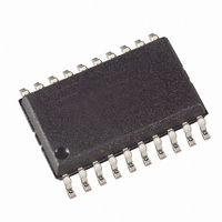
AT90PWM81-16SN Atmel, AT90PWM81-16SN Datasheet - Page 113

AT90PWM81-16SN
Manufacturer Part Number
AT90PWM81-16SN
Description
IC MCU AVR 8K FLASH ISP 20SOIC
Manufacturer
Atmel
Series
AVR® 90PWM Lightingr
Datasheet
1.AT90PWM81-16MN.pdf
(325 pages)
Specifications of AT90PWM81-16SN
Core Processor
AVR
Core Size
8-Bit
Speed
16MHz
Connectivity
SPI
Peripherals
Brown-out Detect/Reset, PWM, WDT
Number Of I /o
16
Program Memory Size
8KB (8K x 8)
Program Memory Type
FLASH
Eeprom Size
512 x 8
Ram Size
256 x 8
Voltage - Supply (vcc/vdd)
2.7 V ~ 5.5 V
Data Converters
A/D 8x10b; D/A 1x10b
Oscillator Type
Internal
Operating Temperature
-40°C ~ 105°C
Package / Case
20-SOIC (7.5mm Width)
Data Bus Width
8 bit
Data Ram Size
256 B
Interface Type
SPI
Maximum Clock Frequency
16 MHz
Number Of Timers
1
Maximum Operating Temperature
+ 105 C
Mounting Style
SMD/SMT
Minimum Operating Temperature
- 40 C
On-chip Adc
10 bit, 8 Channel
On-chip Dac
10 bit, 1 Channel
Height
2.35 mm
Length
13 mm
Supply Voltage (max)
5.5 V
Supply Voltage (min)
2.7 V
Width
7.6 mm
For Use With
ATSTK600-SOIC - STK600 SOCKET/ADAPTER FOR SOIC
Lead Free Status / RoHS Status
Lead free / RoHS Compliant
Available stocks
Company
Part Number
Manufacturer
Quantity
Price
Company:
Part Number:
AT90PWM81-16SN
Manufacturer:
Atmel
Quantity:
1 500
- Current page: 113 of 325
- Download datasheet (6Mb)
12.7.2.2
12.8
7734P–AVR–08/10
PSCOUTn1
PSCOUTn0
Period
PSC Inputs
DT0
Enhanced Mode
OT0
The waveform frequency is defined by the following equation:
The Enhanced Mode uses the previously described method to generate a high resolution frequency.
12-13
Figure 12-13. Enhanced Mode, Timing Diagram
The supplementary step in counting to generate f
frame according to the fractional divider.
page
The waveform frequency is defined by the following equations:
d is the fractional divider factor.
The FWM can be applied on different locations within the PSC output waveforms as defined per
12-15 on page 137
Part A or B of PSC has its own system to take into account one PSC n internal input. Each part A or B is
configured by the PSC n Input A/B Control Register (PFRCnA/B
figuration Register ((see Section “PSC 2 Configuration Register – PCNF2”, page 135)
The PSC input module A is shown on
112.
gives an example of FWM with PBFMn1:0 = 00.
T1
DT1
f
PSCn
f2
OT1
f1
PSCn
=
PSCn
f
AVERAGE
----------------------------- -
PSCnCycle
=
=
-----
T
DT0
1
1
2
Table 12-14
-----
T
1
1
=
=
SeeTable 12-6, “Distribution of fb2 in the modulated frame,” on
=
------------------------------------------------------------------------------
(
----- -
16
OT0
d
-------------------------------------------------------------------- -
(
=
OT0
×
f1
-------------------------------------------------------------------- -
(
+
OT0
PSCn
b2
+
OT1
OT0
OT1
is added on the PSCn0 signal while needed in the
f
f
+
CLK_PSCn
CLK_PSCn
+
+
OT1
16 d
-------------- -
f
+
CLK_PSCn
DT0
16
–
DT0
+
T2
×
+
DT0
f2
page
+
DT1
DT1
PSCn
DT1
+
140) and the PSC n Extended Con-
+
DT1
)
1
)
)
OT1+1
AT90PWM81
DT0
Figure
Table
113
Related parts for AT90PWM81-16SN
Image
Part Number
Description
Manufacturer
Datasheet
Request
R

Part Number:
Description:
Manufacturer:
Atmel Corporation
Datasheet:

Part Number:
Description:
IC MCU AVR 8K FLASH ISP 32QFN
Manufacturer:
Atmel
Datasheet:

Part Number:
Description:
IC MCU AVR 8K FLASH ISP 32QFN
Manufacturer:
Atmel
Datasheet:

Part Number:
Description:
IC MCU AVR 8K FLASH ISP 20SOIC
Manufacturer:
Atmel
Datasheet:

Part Number:
Description:
8-bit Avr Microcontroller With 8k Bytes In- System Programmable Flash
Manufacturer:
ATMEL Corporation
Datasheet:

Part Number:
Description:
DEV KIT FOR AVR/AVR32
Manufacturer:
Atmel
Datasheet:

Part Number:
Description:
INTERVAL AND WIPE/WASH WIPER CONTROL IC WITH DELAY
Manufacturer:
ATMEL Corporation
Datasheet:

Part Number:
Description:
Low-Voltage Voice-Switched IC for Hands-Free Operation
Manufacturer:
ATMEL Corporation
Datasheet:

Part Number:
Description:
MONOLITHIC INTEGRATED FEATUREPHONE CIRCUIT
Manufacturer:
ATMEL Corporation
Datasheet:

Part Number:
Description:
AM-FM Receiver IC U4255BM-M
Manufacturer:
ATMEL Corporation
Datasheet:

Part Number:
Description:
Monolithic Integrated Feature Phone Circuit
Manufacturer:
ATMEL Corporation
Datasheet:

Part Number:
Description:
Multistandard Video-IF and Quasi Parallel Sound Processing
Manufacturer:
ATMEL Corporation
Datasheet:


