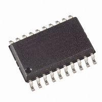
AT90PWM81-16SN Atmel, AT90PWM81-16SN Datasheet - Page 91

AT90PWM81-16SN
Manufacturer Part Number
AT90PWM81-16SN
Description
IC MCU AVR 8K FLASH ISP 20SOIC
Manufacturer
Atmel
Series
AVR® 90PWM Lightingr
Datasheet
1.AT90PWM81-16MN.pdf
(325 pages)
Specifications of AT90PWM81-16SN
Core Processor
AVR
Core Size
8-Bit
Speed
16MHz
Connectivity
SPI
Peripherals
Brown-out Detect/Reset, PWM, WDT
Number Of I /o
16
Program Memory Size
8KB (8K x 8)
Program Memory Type
FLASH
Eeprom Size
512 x 8
Ram Size
256 x 8
Voltage - Supply (vcc/vdd)
2.7 V ~ 5.5 V
Data Converters
A/D 8x10b; D/A 1x10b
Oscillator Type
Internal
Operating Temperature
-40°C ~ 105°C
Package / Case
20-SOIC (7.5mm Width)
Data Bus Width
8 bit
Data Ram Size
256 B
Interface Type
SPI
Maximum Clock Frequency
16 MHz
Number Of Timers
1
Maximum Operating Temperature
+ 105 C
Mounting Style
SMD/SMT
Minimum Operating Temperature
- 40 C
On-chip Adc
10 bit, 8 Channel
On-chip Dac
10 bit, 1 Channel
Height
2.35 mm
Length
13 mm
Supply Voltage (max)
5.5 V
Supply Voltage (min)
2.7 V
Width
7.6 mm
For Use With
ATSTK600-SOIC - STK600 SOCKET/ADAPTER FOR SOIC
Lead Free Status / RoHS Status
Lead free / RoHS Compliant
Available stocks
Company
Part Number
Manufacturer
Quantity
Price
Company:
Part Number:
AT90PWM81-16SN
Manufacturer:
Atmel
Quantity:
1 500
- Current page: 91 of 325
- Download datasheet (6Mb)
11.5
7734P–AVR–08/10
Input Capture Unit
Signal description (internal signals):
The 16-bit counter is mapped into two 8-bit I/O memory locations: Counter High (TCNT1H) containing
the upper eight bits of the counter, and Counter Low (TCNT1L) containing the lower eight bits. The
TCNT1H Register can only be indirectly accessed by the CPU. When the CPU does an access to the
TCNT1H I/O location, the CPU accesses the high byte temporary register (TEMP). The temporary regis-
ter is updated with the TCNT1H value when the TCNT1L is read, and TCNT1H is updated with the
temporary register value when TCNT1L is written. This allows the CPU to read or write the entire 16-bit
counter value within one clock cycle via the 8-bit data bus. It is important to notice that there are special
cases of writing to the TCNT1 Register when the counter is counting that will give unpredictable results.
The special cases are described in the sections where they are of importance.
Depending on the mode of operation used, the counter is cleared, incremented, or decremented at each
timer clock (clk
Clock Select bits (CS12:0). When no clock source is selected (CS12:0 = 0) the timer is stopped. However,
the TCNT1 value can be accessed by the CPU, independent of whether clk
write overrides (has priority over) all counter clear or count operations.
The counting sequence is determined by the setting of the Waveform Generation mode bit (WGM13)
located in the Timer/Counter Control Registers B ( TCCR1B).
The Timer/Counter Overflow Flag (TOV1) is set according to the mode of operation selected by the
WGM13 bit. TOV1 can be used for generating a CPU interrupt.
The Timer/Counter incorporates an Input Capture unit that can capture external events and give them a
time-stamp indicating time of occurrence. The external signal indicating an event, or multiple events, can
be applied via the ICP1 pin or alternatively, via the analog-comparator unit. The time-stamps can then be
used to calculate frequency, duty-cycle, and other features of the signal applied. Alternatively the time-
stamps can be used for creating a log of the events.
The Input Capture unit is illustrated by the block diagram shown in
diagram that are not directly a part of the Input Capture unit are gray shaded. The small “n” in register and
bit names indicates the Timer/Counter number.
Count
Clear
clk
TOP
BOTTOM
T
1
T
1
). The clk
T
1
can be generated from an external or internal clock source, selected by the
Increment TCNT1 by 1.
Clear TCNT1 (set all bits to zero).
Timer/Counter clock.
Signalize that TCNT1 has reached maximum value.
Signalize that TCNT1 has reached minimum value (zero).
Figure
11-4. The elements of the block
T
1
AT90PWM81
is present or not. A CPU
91
Related parts for AT90PWM81-16SN
Image
Part Number
Description
Manufacturer
Datasheet
Request
R

Part Number:
Description:
Manufacturer:
Atmel Corporation
Datasheet:

Part Number:
Description:
IC MCU AVR 8K FLASH ISP 32QFN
Manufacturer:
Atmel
Datasheet:

Part Number:
Description:
IC MCU AVR 8K FLASH ISP 32QFN
Manufacturer:
Atmel
Datasheet:

Part Number:
Description:
IC MCU AVR 8K FLASH ISP 20SOIC
Manufacturer:
Atmel
Datasheet:

Part Number:
Description:
8-bit Avr Microcontroller With 8k Bytes In- System Programmable Flash
Manufacturer:
ATMEL Corporation
Datasheet:

Part Number:
Description:
DEV KIT FOR AVR/AVR32
Manufacturer:
Atmel
Datasheet:

Part Number:
Description:
INTERVAL AND WIPE/WASH WIPER CONTROL IC WITH DELAY
Manufacturer:
ATMEL Corporation
Datasheet:

Part Number:
Description:
Low-Voltage Voice-Switched IC for Hands-Free Operation
Manufacturer:
ATMEL Corporation
Datasheet:

Part Number:
Description:
MONOLITHIC INTEGRATED FEATUREPHONE CIRCUIT
Manufacturer:
ATMEL Corporation
Datasheet:

Part Number:
Description:
AM-FM Receiver IC U4255BM-M
Manufacturer:
ATMEL Corporation
Datasheet:

Part Number:
Description:
Monolithic Integrated Feature Phone Circuit
Manufacturer:
ATMEL Corporation
Datasheet:

Part Number:
Description:
Multistandard Video-IF and Quasi Parallel Sound Processing
Manufacturer:
ATMEL Corporation
Datasheet:


