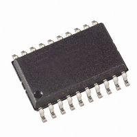
AT90PWM81-16SN Atmel, AT90PWM81-16SN Datasheet - Page 217

AT90PWM81-16SN
Manufacturer Part Number
AT90PWM81-16SN
Description
IC MCU AVR 8K FLASH ISP 20SOIC
Manufacturer
Atmel
Series
AVR® 90PWM Lightingr
Datasheet
1.AT90PWM81-16MN.pdf
(325 pages)
Specifications of AT90PWM81-16SN
Core Processor
AVR
Core Size
8-Bit
Speed
16MHz
Connectivity
SPI
Peripherals
Brown-out Detect/Reset, PWM, WDT
Number Of I /o
16
Program Memory Size
8KB (8K x 8)
Program Memory Type
FLASH
Eeprom Size
512 x 8
Ram Size
256 x 8
Voltage - Supply (vcc/vdd)
2.7 V ~ 5.5 V
Data Converters
A/D 8x10b; D/A 1x10b
Oscillator Type
Internal
Operating Temperature
-40°C ~ 105°C
Package / Case
20-SOIC (7.5mm Width)
Data Bus Width
8 bit
Data Ram Size
256 B
Interface Type
SPI
Maximum Clock Frequency
16 MHz
Number Of Timers
1
Maximum Operating Temperature
+ 105 C
Mounting Style
SMD/SMT
Minimum Operating Temperature
- 40 C
On-chip Adc
10 bit, 8 Channel
On-chip Dac
10 bit, 1 Channel
Height
2.35 mm
Length
13 mm
Supply Voltage (max)
5.5 V
Supply Voltage (min)
2.7 V
Width
7.6 mm
For Use With
ATSTK600-SOIC - STK600 SOCKET/ADAPTER FOR SOIC
Lead Free Status / RoHS Status
Lead free / RoHS Compliant
Available stocks
Company
Part Number
Manufacturer
Quantity
Price
Company:
Part Number:
AT90PWM81-16SN
Manufacturer:
Atmel
Quantity:
1 500
- Current page: 217 of 325
- Download datasheet (6Mb)
7734P–AVR–08/10
• Bit 7, 6 – REFS1, 0: ADC Vref Selection Bits
These 2 bits determine the voltage reference for the ADC and for the other analog devices.
The different setting are shown in
Table 17-3.
If these bits are changed during a conversion, the change will not take effect until this conversion is com-
plete (it means while the ADIF bit in ADCSRA register is set).
In case the internal Vref is selected, it is turned ON as soon as an analog feature needed it is set.
• Bit 5 – ADLAR: ADC Left Adjust Result
Set this bit to left adjust the ADC result.
Clear it to right adjust the ADC result.
The ADLAR bit affects the configuration of the ADC result data registers. Changing this bit affects the
ADC data registers immediately regardless of any on going conversion. For a complete description of this
bit, see Section “ADC Result Data Registers – ADCH and ADCL”, page 220.
• Bit 3, 2, 1, 0 – MUX3, MUX2, MUX1, MUX0: ADC Channel Selection Bits
These 4 bits determine which analog inputs are connected to the ADC input. The different setting are
shown in
Table 17-4.
REFS1
0
0
1
1
MUX3
0
0
0
0
0
0
0
0
1
1
1
1
1
Table
REFS0
0
1
0
1
17-4.
ADC Voltage Reference Selection
ADC Input Channel Selection
MUX2
0
0
0
0
1
1
1
1
0
0
0
0
1
Description
Voltage Reference
External Vref
AVcc
Internal 2.56V Reference voltage
Internal 2.56V Reference voltage
MUX1
0
0
1
1
0
0
1
1
0
0
1
1
0
Table
17-3.
MUX0
0
1
0
1
0
1
0
1
0
1
0
1
0
Description
ADC0
ADC1
ADC2
ADC3
ADC4
ADC5
ADC6
ADC7
ADC8
ADC9
ADC10
AMP0
Temp sensor (Vtemp)
PE3/AREF pin
External Voltage reference
External capacitor for decoupling of the
Internal Reference voltage
PE3 pin free as port
AT90PWM81
217
Related parts for AT90PWM81-16SN
Image
Part Number
Description
Manufacturer
Datasheet
Request
R

Part Number:
Description:
Manufacturer:
Atmel Corporation
Datasheet:

Part Number:
Description:
IC MCU AVR 8K FLASH ISP 32QFN
Manufacturer:
Atmel
Datasheet:

Part Number:
Description:
IC MCU AVR 8K FLASH ISP 32QFN
Manufacturer:
Atmel
Datasheet:

Part Number:
Description:
IC MCU AVR 8K FLASH ISP 20SOIC
Manufacturer:
Atmel
Datasheet:

Part Number:
Description:
8-bit Avr Microcontroller With 8k Bytes In- System Programmable Flash
Manufacturer:
ATMEL Corporation
Datasheet:

Part Number:
Description:
DEV KIT FOR AVR/AVR32
Manufacturer:
Atmel
Datasheet:

Part Number:
Description:
INTERVAL AND WIPE/WASH WIPER CONTROL IC WITH DELAY
Manufacturer:
ATMEL Corporation
Datasheet:

Part Number:
Description:
Low-Voltage Voice-Switched IC for Hands-Free Operation
Manufacturer:
ATMEL Corporation
Datasheet:

Part Number:
Description:
MONOLITHIC INTEGRATED FEATUREPHONE CIRCUIT
Manufacturer:
ATMEL Corporation
Datasheet:

Part Number:
Description:
AM-FM Receiver IC U4255BM-M
Manufacturer:
ATMEL Corporation
Datasheet:

Part Number:
Description:
Monolithic Integrated Feature Phone Circuit
Manufacturer:
ATMEL Corporation
Datasheet:

Part Number:
Description:
Multistandard Video-IF and Quasi Parallel Sound Processing
Manufacturer:
ATMEL Corporation
Datasheet:


