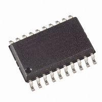
AT90PWM81-16SN Atmel, AT90PWM81-16SN Datasheet - Page 141

AT90PWM81-16SN
Manufacturer Part Number
AT90PWM81-16SN
Description
IC MCU AVR 8K FLASH ISP 20SOIC
Manufacturer
Atmel
Series
AVR® 90PWM Lightingr
Datasheet
1.AT90PWM81-16MN.pdf
(325 pages)
Specifications of AT90PWM81-16SN
Core Processor
AVR
Core Size
8-Bit
Speed
16MHz
Connectivity
SPI
Peripherals
Brown-out Detect/Reset, PWM, WDT
Number Of I /o
16
Program Memory Size
8KB (8K x 8)
Program Memory Type
FLASH
Eeprom Size
512 x 8
Ram Size
256 x 8
Voltage - Supply (vcc/vdd)
2.7 V ~ 5.5 V
Data Converters
A/D 8x10b; D/A 1x10b
Oscillator Type
Internal
Operating Temperature
-40°C ~ 105°C
Package / Case
20-SOIC (7.5mm Width)
Data Bus Width
8 bit
Data Ram Size
256 B
Interface Type
SPI
Maximum Clock Frequency
16 MHz
Number Of Timers
1
Maximum Operating Temperature
+ 105 C
Mounting Style
SMD/SMT
Minimum Operating Temperature
- 40 C
On-chip Adc
10 bit, 8 Channel
On-chip Dac
10 bit, 1 Channel
Height
2.35 mm
Length
13 mm
Supply Voltage (max)
5.5 V
Supply Voltage (min)
2.7 V
Width
7.6 mm
For Use With
ATSTK600-SOIC - STK600 SOCKET/ADAPTER FOR SOIC
Lead Free Status / RoHS Status
Lead free / RoHS Compliant
Available stocks
Company
Part Number
Manufacturer
Quantity
Price
Company:
Part Number:
AT90PWM81-16SN
Manufacturer:
Atmel
Quantity:
1 500
- Current page: 141 of 325
- Download datasheet (6Mb)
7734P–AVR–08/10
The Input Control Registers are used to configure the 2 PSC’s Retrigger/Fault block A & B. The 2 blocks
are identical, so they are configured on the same way.
• Bit 7 – PCAEnx : PSC n Capture Enable Input Part x
Writing this bit to one enables the capture function when external event occurs on input selected as input
for Part x (see PISELnx1:0 bit in the same register).
• Bit 6 – PISELnx0 : PSC n Input Select for Part x
Together with PISELnx1 in PCNFEn register, defines active signal on PSC module A. See
page 138
• Bit 5 –PELEVnx0 : PSC n Edge Level Selector of Input Part x
Together with PELEVnx1 n PCNFEn register, defines active edge & level on PSC part x ; See
16 on page 138
• Bit 4 – PFLTEnx : PSC n Filter Enable on Input Part x
Setting this bit (to one) activates the Input Capture Noise Canceler. When the noise canceler is activated,
the input from the retrigger pin is filtered. The filter function requires four successive equal valued sam-
ples of the retrigger pin for changing its output. The Input Capture is therefore delayed by four oscillator
cycles when the noise canceler is enabled.
• Bit 3:0 – PRFMnx3:0: PSC n Fault Mode
These four bits define the mode of operation of the Fault or Retrigger functions.
(see PSC Functional Specification for more explanations)
Table 12-21.
PRFMnx3:0
0000b
0001b
0010b
0011b
0100b
0101b
0110b
0111b
1000b
1001b
and
Table 12-19 on page 139
and
Level Sensitivity and Fault Mode Operation
Description
No action, PSC Input is ignored
PSC Input Mode 1: Stop signal, Jump to Opposite Dead-Time and Wait
PSC Input Mode 2: Stop signal, Execute Opposite Pulse and Wait
PSC Input Mode 3: Stop signal, Execute Opposite Pulse while Fault active
PSC Input Mode 4: Deactivate outputs without changing timing.
PSC Input Mode 5: Stop signal and Insert Dead-Time
PSC Input Mode 6: Stop signal, Jump to Opposite Dead-Time and Wait.
PSC Input Mode 7: Halt PSC and Wait for Software Action
PSC Input Mode 8: Edge Retrigger PSC
PSC Input Mode 9: Fixed Frequency Edge Retrigger PSC
Table 12-17 on page 138
AT90PWM81
Table 12-18 on
Table 12-
141
Related parts for AT90PWM81-16SN
Image
Part Number
Description
Manufacturer
Datasheet
Request
R

Part Number:
Description:
Manufacturer:
Atmel Corporation
Datasheet:

Part Number:
Description:
IC MCU AVR 8K FLASH ISP 32QFN
Manufacturer:
Atmel
Datasheet:

Part Number:
Description:
IC MCU AVR 8K FLASH ISP 32QFN
Manufacturer:
Atmel
Datasheet:

Part Number:
Description:
IC MCU AVR 8K FLASH ISP 20SOIC
Manufacturer:
Atmel
Datasheet:

Part Number:
Description:
8-bit Avr Microcontroller With 8k Bytes In- System Programmable Flash
Manufacturer:
ATMEL Corporation
Datasheet:

Part Number:
Description:
DEV KIT FOR AVR/AVR32
Manufacturer:
Atmel
Datasheet:

Part Number:
Description:
INTERVAL AND WIPE/WASH WIPER CONTROL IC WITH DELAY
Manufacturer:
ATMEL Corporation
Datasheet:

Part Number:
Description:
Low-Voltage Voice-Switched IC for Hands-Free Operation
Manufacturer:
ATMEL Corporation
Datasheet:

Part Number:
Description:
MONOLITHIC INTEGRATED FEATUREPHONE CIRCUIT
Manufacturer:
ATMEL Corporation
Datasheet:

Part Number:
Description:
AM-FM Receiver IC U4255BM-M
Manufacturer:
ATMEL Corporation
Datasheet:

Part Number:
Description:
Monolithic Integrated Feature Phone Circuit
Manufacturer:
ATMEL Corporation
Datasheet:

Part Number:
Description:
Multistandard Video-IF and Quasi Parallel Sound Processing
Manufacturer:
ATMEL Corporation
Datasheet:


