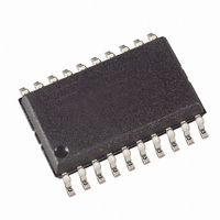
AT90PWM81-16SN Atmel, AT90PWM81-16SN Datasheet - Page 28

AT90PWM81-16SN
Manufacturer Part Number
AT90PWM81-16SN
Description
IC MCU AVR 8K FLASH ISP 20SOIC
Manufacturer
Atmel
Series
AVR® 90PWM Lightingr
Datasheet
1.AT90PWM81-16MN.pdf
(325 pages)
Specifications of AT90PWM81-16SN
Core Processor
AVR
Core Size
8-Bit
Speed
16MHz
Connectivity
SPI
Peripherals
Brown-out Detect/Reset, PWM, WDT
Number Of I /o
16
Program Memory Size
8KB (8K x 8)
Program Memory Type
FLASH
Eeprom Size
512 x 8
Ram Size
256 x 8
Voltage - Supply (vcc/vdd)
2.7 V ~ 5.5 V
Data Converters
A/D 8x10b; D/A 1x10b
Oscillator Type
Internal
Operating Temperature
-40°C ~ 105°C
Package / Case
20-SOIC (7.5mm Width)
Data Bus Width
8 bit
Data Ram Size
256 B
Interface Type
SPI
Maximum Clock Frequency
16 MHz
Number Of Timers
1
Maximum Operating Temperature
+ 105 C
Mounting Style
SMD/SMT
Minimum Operating Temperature
- 40 C
On-chip Adc
10 bit, 8 Channel
On-chip Dac
10 bit, 1 Channel
Height
2.35 mm
Length
13 mm
Supply Voltage (max)
5.5 V
Supply Voltage (min)
2.7 V
Width
7.6 mm
For Use With
ATSTK600-SOIC - STK600 SOCKET/ADAPTER FOR SOIC
Lead Free Status / RoHS Status
Lead free / RoHS Compliant
Available stocks
Company
Part Number
Manufacturer
Quantity
Price
Company:
Part Number:
AT90PWM81-16SN
Manufacturer:
Atmel
Quantity:
1 500
- Current page: 28 of 325
- Download datasheet (6Mb)
5.1.1
5.1.2
5.1.3
5.1.4
5.1.5
5.2
Table 5-1.
28
Device Clocking Option
External Clock
PLL output divided by 4 : 16 MHz driven by internal RC
Calibrated Internal RC Oscillator 8 MHz
Internal 128 kHz RC Oscillator (WD)
PLL output divided by 4 / PLL driven by External
Crystal/Ceramic Resonator
PLL output divided by 4/ PLL driven by External clock
Calibrated Internal RC Oscillator 1MHz
External Crystal/Ceramic Resonator (3.0 - 8.0 MHz)
External Crystal/Ceramic Resonator (0.9 - 3.0 MHz)
External Crystal/Ceramic Resonator (0.9 - 3.0 MHz)
External Crystal/Ceramic Resonator (3.0 - 8.0 MHz)
External Crystal/Ceramic Resonator (3.0 - 8.0 MHz)
Clock Sources
AT90PWM81
CPU Clock – clk
I/O Clock – clk
Flash Clock – clk
PLL Clock – clk
ADC Clock – clk
Device Clocking Options Select
I/O
PLL
The CPU clock is routed to parts of the system concerned with operation of the AVR core. Examples of
such modules are the General Purpose Register File, the Status Register and the Data memory holding the
Stack Pointer. Halting the CPU clock inhibits the core from performing general operations and
calculations.
The I/O clock is used by the majority of the I/O modules, like Timer/Counter. The I/O clock is also used
by the External Interrupt module, but note that some external interrupts are detected by asynchronous
logic, allowing such interrupts to be detected even if the I/O clock is halted.
The Flash clock controls operation of the Flash interface. The Flash clock is usually active simultaneously
with the CPU clock.
The PLL clock allows the PSC modules to be clocked directly from a 64/32 MHz clock. A 16 MHz clock
is also derived for the CPU.
The ADC is provided with a dedicated clock domain. This allows halting the CPU and I/O clocks in order
to reduce noise generated by digital circuitry. This gives more accurate ADC conversion results.
The device has the following clock source options, selectable by Flash Fuse bits (default) or by the CLK-
SELR register (dynamic clock switch circuit) as shown below. The clock from the selected source is input
to the AVR clock generator, and routed to the appropriate modules.
CPU
ADC
FLASH
(1)
, PLL source and PE1 and PE2 functionality
System
Clock
Ext Clk
PLL / 4
RC Osc
WD
PLL / 4
PLL / 4
RC Osc
Ext Osc
Ext Osc
Ext Osc
Ext Osc
Ext Osc
PLL Input
RC Osc
RC Osc
Ext Osc
RC Osc
N/A
Ext Clk
N/A
Ext Osc
RC Osc
RC Osc
RC Osc
RC Osc
(2)
CKSEL3..0
CSEL3..0
0111
1000
1001
1010
1011
0000
0001
0010
0011
0101
0110
0100
b
b
b
b
b
(4)
(3)
XTAL1
XTAL1
XTAL1
XTAL1
XTAL1
XTAL1
CLKI
CLKI
PE1
I/O
I/O
I/O
I/O
7734P–AVR–08/10
XTAL2
XTAL2
XTAL2
XTAL2
XTAL2
XTAL2
PE2
I/O
I/O
I/O
I/O
I/O
I/O
Related parts for AT90PWM81-16SN
Image
Part Number
Description
Manufacturer
Datasheet
Request
R

Part Number:
Description:
Manufacturer:
Atmel Corporation
Datasheet:

Part Number:
Description:
IC MCU AVR 8K FLASH ISP 32QFN
Manufacturer:
Atmel
Datasheet:

Part Number:
Description:
IC MCU AVR 8K FLASH ISP 32QFN
Manufacturer:
Atmel
Datasheet:

Part Number:
Description:
IC MCU AVR 8K FLASH ISP 20SOIC
Manufacturer:
Atmel
Datasheet:

Part Number:
Description:
8-bit Avr Microcontroller With 8k Bytes In- System Programmable Flash
Manufacturer:
ATMEL Corporation
Datasheet:

Part Number:
Description:
DEV KIT FOR AVR/AVR32
Manufacturer:
Atmel
Datasheet:

Part Number:
Description:
INTERVAL AND WIPE/WASH WIPER CONTROL IC WITH DELAY
Manufacturer:
ATMEL Corporation
Datasheet:

Part Number:
Description:
Low-Voltage Voice-Switched IC for Hands-Free Operation
Manufacturer:
ATMEL Corporation
Datasheet:

Part Number:
Description:
MONOLITHIC INTEGRATED FEATUREPHONE CIRCUIT
Manufacturer:
ATMEL Corporation
Datasheet:

Part Number:
Description:
AM-FM Receiver IC U4255BM-M
Manufacturer:
ATMEL Corporation
Datasheet:

Part Number:
Description:
Monolithic Integrated Feature Phone Circuit
Manufacturer:
ATMEL Corporation
Datasheet:

Part Number:
Description:
Multistandard Video-IF and Quasi Parallel Sound Processing
Manufacturer:
ATMEL Corporation
Datasheet:


