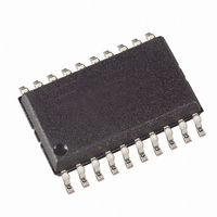
AT90PWM81-16SN Atmel, AT90PWM81-16SN Datasheet - Page 256

AT90PWM81-16SN
Manufacturer Part Number
AT90PWM81-16SN
Description
IC MCU AVR 8K FLASH ISP 20SOIC
Manufacturer
Atmel
Series
AVR® 90PWM Lightingr
Datasheet
1.AT90PWM81-16MN.pdf
(325 pages)
Specifications of AT90PWM81-16SN
Core Processor
AVR
Core Size
8-Bit
Speed
16MHz
Connectivity
SPI
Peripherals
Brown-out Detect/Reset, PWM, WDT
Number Of I /o
16
Program Memory Size
8KB (8K x 8)
Program Memory Type
FLASH
Eeprom Size
512 x 8
Ram Size
256 x 8
Voltage - Supply (vcc/vdd)
2.7 V ~ 5.5 V
Data Converters
A/D 8x10b; D/A 1x10b
Oscillator Type
Internal
Operating Temperature
-40°C ~ 105°C
Package / Case
20-SOIC (7.5mm Width)
Data Bus Width
8 bit
Data Ram Size
256 B
Interface Type
SPI
Maximum Clock Frequency
16 MHz
Number Of Timers
1
Maximum Operating Temperature
+ 105 C
Mounting Style
SMD/SMT
Minimum Operating Temperature
- 40 C
On-chip Adc
10 bit, 8 Channel
On-chip Dac
10 bit, 1 Channel
Height
2.35 mm
Length
13 mm
Supply Voltage (max)
5.5 V
Supply Voltage (min)
2.7 V
Width
7.6 mm
For Use With
ATSTK600-SOIC - STK600 SOCKET/ADAPTER FOR SOIC
Lead Free Status / RoHS Status
Lead free / RoHS Compliant
Available stocks
Company
Part Number
Manufacturer
Quantity
Price
Company:
Part Number:
AT90PWM81-16SN
Manufacturer:
Atmel
Quantity:
1 500
- Current page: 256 of 325
- Download datasheet (6Mb)
21.7.4
256
AT90PWM81
Programming the Flash
The Flash is organized in pages, see
data is latched into a page buffer. This allows one page of program data to be programmed simultane-
ously. The following procedure describes how to program the entire Flash memory:
A. Load Command “Write Flash”
B. Load Address Low byte
C. Load Data Low Byte
D. Load Data High Byte
E. Latch Data
F. Repeat B through E until the entire buffer is filled or until all data within the page is loaded.
While the lower bits in the address are mapped to words within the page, the higher bits address the pages
within the FLASH. This is illustrated in
required to address words in the page (pagesize < 256), the most significant bit(s) in the address low byte
are used to address the page when performing a Page Write.
G. Load Address High byte
H. Program Page
I. Repeat B through H until the entire Flash is programmed or until all data has been programmed.
1.
2.
3.
4.
1.
2.
3.
4.
1.
2.
3.
1.
2.
3.
4.
1.
2.
1.
2.
3.
4.
1.
2.
Set XA1, XA0 to “10”. This enables command loading.
Set BS1 to “0”.
Set DATA to “0001 0000”. This is the command for Write Flash.
Give XTAL1 a positive pulse. This loads the command.
Set XA1, XA0 to “00”. This enables address loading.
Set BS1 to “0”. This selects low address.
Set DATA = Address low byte (0x00 - 0xFF).
Give XTAL1 a positive pulse. This loads the address low byte.
Set XA1, XA0 to “01”. This enables data loading.
Set DATA = Data low byte (0x00 - 0xFF).
Give XTAL1 a positive pulse. This loads the data byte.
Set BS1 to “1”. This selects high data byte.
Set XA1, XA0 to “01”. This enables data loading.
Set DATA = Data high byte (0x00 - 0xFF).
Give XTAL1 a positive pulse. This loads the data byte.
Set BS1 to “1”. This selects high data byte.
Give PAGEL a positive pulse. This latches the data bytes. (See
waveforms)
Set XA1, XA0 to “00”. This enables address loading.
Set BS1 to “1”. This selects high address.
Set DATA = Address high byte (0x00 - 0xFF).
Give XTAL1 a positive pulse. This loads the address high byte.
Give WR a negative pulse. This starts programming of the entire page of data. RDY/BSY goes
low.
Wait until RDY/BSY goes high (See
Table 21-11 on page
Figure 21-2 on page
Figure 21-3
for signal waveforms).
254. When programming the Flash, the program
257. Note that if less than eight bits are
Figure 21-3
for signal
7734P–AVR–08/10
Related parts for AT90PWM81-16SN
Image
Part Number
Description
Manufacturer
Datasheet
Request
R

Part Number:
Description:
Manufacturer:
Atmel Corporation
Datasheet:

Part Number:
Description:
IC MCU AVR 8K FLASH ISP 32QFN
Manufacturer:
Atmel
Datasheet:

Part Number:
Description:
IC MCU AVR 8K FLASH ISP 32QFN
Manufacturer:
Atmel
Datasheet:

Part Number:
Description:
IC MCU AVR 8K FLASH ISP 20SOIC
Manufacturer:
Atmel
Datasheet:

Part Number:
Description:
8-bit Avr Microcontroller With 8k Bytes In- System Programmable Flash
Manufacturer:
ATMEL Corporation
Datasheet:

Part Number:
Description:
DEV KIT FOR AVR/AVR32
Manufacturer:
Atmel
Datasheet:

Part Number:
Description:
INTERVAL AND WIPE/WASH WIPER CONTROL IC WITH DELAY
Manufacturer:
ATMEL Corporation
Datasheet:

Part Number:
Description:
Low-Voltage Voice-Switched IC for Hands-Free Operation
Manufacturer:
ATMEL Corporation
Datasheet:

Part Number:
Description:
MONOLITHIC INTEGRATED FEATUREPHONE CIRCUIT
Manufacturer:
ATMEL Corporation
Datasheet:

Part Number:
Description:
AM-FM Receiver IC U4255BM-M
Manufacturer:
ATMEL Corporation
Datasheet:

Part Number:
Description:
Monolithic Integrated Feature Phone Circuit
Manufacturer:
ATMEL Corporation
Datasheet:

Part Number:
Description:
Multistandard Video-IF and Quasi Parallel Sound Processing
Manufacturer:
ATMEL Corporation
Datasheet:


