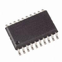
AT90PWM81-16SN Atmel, AT90PWM81-16SN Datasheet - Page 85

AT90PWM81-16SN
Manufacturer Part Number
AT90PWM81-16SN
Description
IC MCU AVR 8K FLASH ISP 20SOIC
Manufacturer
Atmel
Series
AVR® 90PWM Lightingr
Datasheet
1.AT90PWM81-16MN.pdf
(325 pages)
Specifications of AT90PWM81-16SN
Core Processor
AVR
Core Size
8-Bit
Speed
16MHz
Connectivity
SPI
Peripherals
Brown-out Detect/Reset, PWM, WDT
Number Of I /o
16
Program Memory Size
8KB (8K x 8)
Program Memory Type
FLASH
Eeprom Size
512 x 8
Ram Size
256 x 8
Voltage - Supply (vcc/vdd)
2.7 V ~ 5.5 V
Data Converters
A/D 8x10b; D/A 1x10b
Oscillator Type
Internal
Operating Temperature
-40°C ~ 105°C
Package / Case
20-SOIC (7.5mm Width)
Data Bus Width
8 bit
Data Ram Size
256 B
Interface Type
SPI
Maximum Clock Frequency
16 MHz
Number Of Timers
1
Maximum Operating Temperature
+ 105 C
Mounting Style
SMD/SMT
Minimum Operating Temperature
- 40 C
On-chip Adc
10 bit, 8 Channel
On-chip Dac
10 bit, 1 Channel
Height
2.35 mm
Length
13 mm
Supply Voltage (max)
5.5 V
Supply Voltage (min)
2.7 V
Width
7.6 mm
For Use With
ATSTK600-SOIC - STK600 SOCKET/ADAPTER FOR SOIC
Lead Free Status / RoHS Status
Lead free / RoHS Compliant
Available stocks
Company
Part Number
Manufacturer
Quantity
Price
Company:
Part Number:
AT90PWM81-16SN
Manufacturer:
Atmel
Quantity:
1 500
- Current page: 85 of 325
- Download datasheet (6Mb)
11.1.1
7734P–AVR–08/10
Registers
Figure 11-1.
Note:
The Timer/Counter (TCNT1), and Input Capture Register (ICR1) are all 16-bit registers. Special proce-
dures must be followed when accessing the 16-bit registers. These procedures are described in the section
“Accessing 16-bit Registers” on page
registers and have no CPU access restrictions. Interrupt requests (abbreviated to Int.Req. in the figure) sig-
nals are all visible in the Timer Interrupt Flag Register (TIFR1). All interrupts are individually masked
with the Timer Interrupt Mask Register (TIMSK1). TIFR1 and TIMSK1 are not shown in the figure.
The Timer/Counter can be clocked internally, or by an external clock source on the T1 pin. The Clock
Select logic block controls which clock source and edge the Timer/Counter uses to increment (or decre-
ment) its value. The Timer/Counter is inactive when no clock source is selected. The output from the
Clock Select logic is referred to as the timer clock (clk
The Input Capture Register can capture the Timer/Counter value at a given external (edge triggered) event
on either the Input Capture pin (ICP1). The Input Capture unit includes a digital filtering unit (Noise Can-
celer) for reducing the chance of capturing noise spikes.
The TOP value, or maximum Timer/Counter value, can in some modes of operation be defined by the
ICR1 Register, or by a set of fixed values.
1. Refer to
16-bit Timer/Counter Block Diagram
Table 2-1 on page 5
Timer/Counter
TCNTn
ICRn
Count
Clear
86. The Timer/Counter Control Registers (TCCR1A/B) are 8-bit
for Timer/Counter1 pin placement and description.
Control Logic
TOP
=
TCCRnB
Values
BOTTOM
(1)
Fixed
TOP
T
ICFn (Int.Req.)
1
).
clk
Detector
Edge
=
Tn
0
TOVn
(Int.Req.)
Clock Select
(Ckio )
Canceler
Detector
Noise
Edge
AT90PWM81
Comparator Ouput )
AC1ICE
( From Analog
ICPn
Tn
85
Related parts for AT90PWM81-16SN
Image
Part Number
Description
Manufacturer
Datasheet
Request
R

Part Number:
Description:
Manufacturer:
Atmel Corporation
Datasheet:

Part Number:
Description:
IC MCU AVR 8K FLASH ISP 32QFN
Manufacturer:
Atmel
Datasheet:

Part Number:
Description:
IC MCU AVR 8K FLASH ISP 32QFN
Manufacturer:
Atmel
Datasheet:

Part Number:
Description:
IC MCU AVR 8K FLASH ISP 20SOIC
Manufacturer:
Atmel
Datasheet:

Part Number:
Description:
8-bit Avr Microcontroller With 8k Bytes In- System Programmable Flash
Manufacturer:
ATMEL Corporation
Datasheet:

Part Number:
Description:
DEV KIT FOR AVR/AVR32
Manufacturer:
Atmel
Datasheet:

Part Number:
Description:
INTERVAL AND WIPE/WASH WIPER CONTROL IC WITH DELAY
Manufacturer:
ATMEL Corporation
Datasheet:

Part Number:
Description:
Low-Voltage Voice-Switched IC for Hands-Free Operation
Manufacturer:
ATMEL Corporation
Datasheet:

Part Number:
Description:
MONOLITHIC INTEGRATED FEATUREPHONE CIRCUIT
Manufacturer:
ATMEL Corporation
Datasheet:

Part Number:
Description:
AM-FM Receiver IC U4255BM-M
Manufacturer:
ATMEL Corporation
Datasheet:

Part Number:
Description:
Monolithic Integrated Feature Phone Circuit
Manufacturer:
ATMEL Corporation
Datasheet:

Part Number:
Description:
Multistandard Video-IF and Quasi Parallel Sound Processing
Manufacturer:
ATMEL Corporation
Datasheet:


