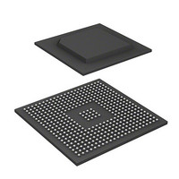
R8A77850ADBGV#RD0Z Renesas Electronics America, R8A77850ADBGV#RD0Z Datasheet - Page 293

R8A77850ADBGV#RD0Z
Manufacturer Part Number
R8A77850ADBGV#RD0Z
Description
IC SUPERH MPU ROMLESS 436-BGA
Manufacturer
Renesas Electronics America
Series
SuperH® SH7780r
Datasheet
1.R8A77850AADBGV.pdf
(1694 pages)
Specifications of R8A77850ADBGV#RD0Z
Core Processor
SH-4A
Core Size
32-Bit
Speed
600MHz
Connectivity
Audio Codec, MMC, Serial Sound, SCI, SIO, SPI, SSI
Peripherals
DMA, POR, WDT
Number Of I /o
108
Program Memory Type
ROMless
Ram Size
8K x 8
Voltage - Supply (vcc/vdd)
1 V ~ 1.2 V
Oscillator Type
External
Operating Temperature
-40°C ~ 85°C
Package / Case
436-BGA
Lead Free Status / RoHS Status
Lead free / RoHS Compliant
Eeprom Size
-
Program Memory Size
-
Data Converters
-
Available stocks
Company
Part Number
Manufacturer
Quantity
Price
Part Number:
R8A77850ADBGV#RD0ZR8A77850ADBGV
Manufacturer:
Renesas Electronics America
Quantity:
10 000
- Current page: 293 of 1694
- Download datasheet (9Mb)
9.5
9.5.1
In the event of simultaneous access to the same page from different buses, page conflict occurs.
Although each access is completed correctly, this kind of conflict tends to lower OL memory
accessibility. Therefore it is advisable to provide all possible preventative software measures. For
example, conflicts will not occur if each bus accesses different pages.
9.5.2
(1)
Read access from the operand bus is performed in one cycle when the access is made successively
to the same page but takes multiple cycles (a maximum of two wait cycles may be required) when
the access is made across pages or the previous access was made to memory other than OL
memory. For this reason, from the viewpoint of performance optimization, it is recommended to
design the software such that the page corresponding to the address for read access from the
operand bus does not change so often.
(2)
Access from the instruction bus is performed in one cycle when the access is made successively to
the same page but takes multiple cycles (a maximum of two wait cycles may be required) when
the access is made across pages or the previous access was made to memory other than IL
memory. For this reason, from the viewpoint of performance optimization, it is recommended to
design the software such that the target page does not change so often in access from the
instruction bus. For example, allocating a separate program for each page will deliver better
efficiency.
9.5.3
(1)
In order to allocate instructions in the OL memory, write an instruction to the OL memory,
execute the following sequence, then branch to the rewritten instruction.
• SYNCO
• ICBI @Rn
In this case, the target for the ICBI instruction can be any address (OL memory address may be
possible) within the range where no address error exception occurs, and cache hit/miss is possible.
OL Memory
IL Memory
OL Memory
Usage Notes
Page Conflict
Access Across Different Pages
On-Chip Memory Coherency
Rev.1.00 Jan. 10, 2008 Page 261 of 1658
9. On-Chip Memory
REJ09B0261-0100
Related parts for R8A77850ADBGV#RD0Z
Image
Part Number
Description
Manufacturer
Datasheet
Request
R

Part Number:
Description:
KIT STARTER FOR M16C/29
Manufacturer:
Renesas Electronics America
Datasheet:

Part Number:
Description:
KIT STARTER FOR R8C/2D
Manufacturer:
Renesas Electronics America
Datasheet:

Part Number:
Description:
R0K33062P STARTER KIT
Manufacturer:
Renesas Electronics America
Datasheet:

Part Number:
Description:
KIT STARTER FOR R8C/23 E8A
Manufacturer:
Renesas Electronics America
Datasheet:

Part Number:
Description:
KIT STARTER FOR R8C/25
Manufacturer:
Renesas Electronics America
Datasheet:

Part Number:
Description:
KIT STARTER H8S2456 SHARPE DSPLY
Manufacturer:
Renesas Electronics America
Datasheet:

Part Number:
Description:
KIT STARTER FOR R8C38C
Manufacturer:
Renesas Electronics America
Datasheet:

Part Number:
Description:
KIT STARTER FOR R8C35C
Manufacturer:
Renesas Electronics America
Datasheet:

Part Number:
Description:
KIT STARTER FOR R8CL3AC+LCD APPS
Manufacturer:
Renesas Electronics America
Datasheet:

Part Number:
Description:
KIT STARTER FOR RX610
Manufacturer:
Renesas Electronics America
Datasheet:

Part Number:
Description:
KIT STARTER FOR R32C/118
Manufacturer:
Renesas Electronics America
Datasheet:

Part Number:
Description:
KIT DEV RSK-R8C/26-29
Manufacturer:
Renesas Electronics America
Datasheet:

Part Number:
Description:
KIT STARTER FOR SH7124
Manufacturer:
Renesas Electronics America
Datasheet:

Part Number:
Description:
KIT STARTER FOR H8SX/1622
Manufacturer:
Renesas Electronics America
Datasheet:

Part Number:
Description:
KIT DEV FOR SH7203
Manufacturer:
Renesas Electronics America
Datasheet:


