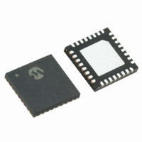
MRF89XA-I/MQ Microchip Technology, MRF89XA-I/MQ Datasheet - Page 15

MRF89XA-I/MQ
Manufacturer Part Number
MRF89XA-I/MQ
Description
TXRX ISM SUB-GHZ ULP 32QFN
Manufacturer
Microchip Technology
Specifications of MRF89XA-I/MQ
Package / Case
32-WFQFN Exposed Pad
Frequency
863MHz ~ 870MHz, 902MHz ~ 928MHz, 950MHz ~ 960MHz
Data Rate - Maximum
200kbps
Modulation Or Protocol
FSK, OOK
Applications
ISM
Power - Output
12.5dBm
Sensitivity
-113dBm
Voltage - Supply
2.1 V ~ 3.6 V
Current - Receiving
3mA
Current - Transmitting
25mA
Data Interface
PCB, Surface Mount
Antenna Connector
PCB, Surface Mount
Operating Temperature
-40°C ~ 85°C
Number Of Receivers
1
Number Of Transmitters
1
Wireless Frequency
863 MHz to 870 MHz, 902 MHz to 928 MHz, 950 MHz to 960 MHz
Interface Type
SPI
Noise Figure
- 112 dBc
Output Power
- 8.5 dBm, + 12.5 dBm
Operating Supply Voltage
2.1 V to 3.6 V
Maximum Operating Temperature
+ 85 C
Mounting Style
SMD/SMT
Maximum Data Rate
256 Kbps
Maximum Supply Current
25 mA
Minimum Operating Temperature
- 40 C
Modulation
FSK
Lead Free Status / RoHS Status
Lead free / RoHS Compliant
Memory Size
-
Lead Free Status / Rohs Status
Lead free / RoHS Compliant
Available stocks
Company
Part Number
Manufacturer
Quantity
Price
Company:
Part Number:
MRF89XA-I/MQ
Manufacturer:
MICROCHIP
Quantity:
12 000
2.2
The device enters the Reset mode if any of the
following events take place:
• Power-on Reset (POR)
• Manual Reset
The POR happens when the MRF89XA is switched on
using V
execute any communication operations on the SPI bus.
An external hardware or manual Reset of the
MRF89XA can be performed by asserting the TEST8
pin (pin 13) to high for 100 µs and then releasing the
pin. After releasing the pin, it takes more than 5 ms for
the transceiver to be ready for any operations. The pin
is driven with an open-drain output, and therefore, is
pulled high while the device is in POR. The device will
not accept commands during the Reset period. For
more information, refer to Section 3.1.2 “Manual
Reset”.
2.3
The receiver and the transmitter share the same RFIO
pin (pin 31). Figure 2-3 illustrates the configuration of
the common RF front-end.
• In Transmit mode, the PA and the PA regulator
• In Receive mode, the PA and PA regulator are
FIGURE 2-3:
© 2010 Microchip Technology Inc.
are ON, with voltage on the PARS pin (pin 29)
equal to the nominal voltage of the regulator
(about 1.8V). The external RF choke inductance
is used to bias the PA.
OFF and PARS is tied to ground. The external RF
choke inductor is then used for biasing and
matching the LNA (this is basically implemented
as a common gate amplifier).
To
Antenna
DD
Reset Pin
RFIO Pin
. The POR cycle takes at least 10 ms to
PARS
RFIO
COMMON RF INPUT AND
OUTPUT PIN DIAGRAM
RX ON
PA Regulator
(1.8V)
LNA
PA
Preliminary
The PA and the LNA front-ends in the MRF89XA, which
share the same Input/Output pin, are internally
matched to approximately 50Ω.
2.4
2.4.1
After digital-to-analog conversion during transmission,
both I and Q signals are smoothed by interpolation
filters. These low-pass filters the digitally generated
signal, and prevents the alias signals from entering the
modulators.
2.4.2
The Power Amplifier (PA) integrated in the MRF89XA
operates under a regulated voltage supply of 1.8V. The
external RF choke inductor is biased by an internal
29). Therefore, the PA output power is consistent over
the power supply range. This is important for
applications
performance and battery life.
An open collector output requires biasing using an
inductor as an RF choke. For the recommended PA
bias and matching circuit details see Section 4.4.2
“Suggested PA Biasing And Matching”.
The matching of the SAW filter depends on the SAW
filter selected. Many modern SAW filters have 50Ω
input and output, which simplifies matching for the
MRF89XA. This is demonstrated in the application
circuit. If the choice of SAW filter is different than 50Ω,
the required impedance match on the input and output
of the SAW filter will be needed.
2.4.3
In Receive mode, the RFIO pin (pin 31) is connected to
a fixed gain, common-gate, Low Noise Amplifier (LNA).
The performance of this amplifier is such that the Noise
Figure (NF) of the receiver is estimated to be
approximately 7 dB.
The LNA has approximately 50Ω impedance, which
functions
(PCB/Monopole) during signal transmission. The LNA
is followed by an internal RF band-pass filter.
regulator output made available on the PARS pin (pin
Note:
Filters and Amplifiers Block
INTERPOLATION FILTER
POWER AMPLIFIER
For applications, it is recommended that
an appropriate SAW filter needs to be
implemented.
LOW
FIRST MIXER)
well
which
with
NOISE
allows
the
MRF89XA
AMPLIFIER
both
proposed
DS70622B-page 15
predictable
antenna
(WITH
RF


