MRF89XA-I/MQ Microchip Technology, MRF89XA-I/MQ Datasheet - Page 98
MRF89XA-I/MQ
Manufacturer Part Number
MRF89XA-I/MQ
Description
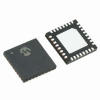
TXRX ISM SUB-GHZ ULP 32QFN
Manufacturer
Microchip Technology
Specifications of MRF89XA-I/MQ
Package / Case
32-WFQFN Exposed Pad
Frequency
863MHz ~ 870MHz, 902MHz ~ 928MHz, 950MHz ~ 960MHz
Data Rate - Maximum
200kbps
Modulation Or Protocol
FSK, OOK
Applications
ISM
Power - Output
12.5dBm
Sensitivity
-113dBm
Voltage - Supply
2.1 V ~ 3.6 V
Current - Receiving
3mA
Current - Transmitting
25mA
Data Interface
PCB, Surface Mount
Antenna Connector
PCB, Surface Mount
Operating Temperature
-40°C ~ 85°C
Number Of Receivers
1
Number Of Transmitters
1
Wireless Frequency
863 MHz to 870 MHz, 902 MHz to 928 MHz, 950 MHz to 960 MHz
Interface Type
SPI
Noise Figure
- 112 dBc
Output Power
- 8.5 dBm, + 12.5 dBm
Operating Supply Voltage
2.1 V to 3.6 V
Maximum Operating Temperature
+ 85 C
Mounting Style
SMD/SMT
Maximum Data Rate
256 Kbps
Maximum Supply Current
25 mA
Minimum Operating Temperature
- 40 C
Modulation
FSK
Lead Free Status / RoHS Status
Lead free / RoHS Compliant
Memory Size
-
Lead Free Status / Rohs Status
Lead free / RoHS Compliant
Available stocks
Company
Part Number
Manufacturer
Quantity
Price
Company:

Part Number:
MRF89XA-I/MQ
Manufacturer:
MICROCHIP
Quantity:
12 000


4.1
The optimum load for the RF port at a given frequency
band is listed in Table 4-1. These load values in the
table are expected by the RF port pins to have as an
antenna load for maximum power transfer. For all
antenna applications, an RF choke inductor (L2) must
be included during transmission because the RF out-
puts are of open-collector type.
4.2
The MRF89XA is single-ended and has an unbalanced
input/output impedance close to 30-j25. Therefore, it
only requires a matching circuit to the SAW filter and
antenna. C11, C12, and L6, L1, C4, and C5 are tuned
to provide that impedance (30+j25) to the RFIO pin
(pin 31). In this case, the transceiver will be able to
transfer all power toward the antenna. This impedance
is called Optimum Load Impedance. L2 is a RF choke
inductor. L3 and L4 are basically VCO inductors. The
details are shown in Figure 4-1.
TABLE 4-1:
DS70622B-page 98
MRF89XA
868 MHz TA0801A
915 MHz TA0281A
Band
RF Transmitter Matching
Antenna Components
FL1
ANTENNA LOAD VALUES
FOR 868 MHz AND 915 MHz
FREQUENCY BANDS
1.8 pF
1.8 pF
C5
22 pF
30 pF
C4
8.2 nH
10 nH
L1
Preliminary
4.3
FL1 is a SAW filter. While in Transmitting mode, the
SAW filter is used to suppress the harmonics. While in
Receiving mode, the SAW filter is used to reject the
image frequencies and out-of-band interfering signals.
4.3.1
Figure 4-2 and Figure 4-3 illustrates the plots of the
SAW filter used in the application circuit. The plots
shown are representative. For exact specifications,
refer to the SAW Filter manufacturer data sheet.
SAW FILTER
SAW FILTER PLOT
© 2010 Microchip Technology Inc.
Related parts for MRF89XA-I/MQ
Image
Part Number
Description
Manufacturer
Datasheet
Request
R

Part Number:
Description:
Ultra-low Power, Integrated Ism Band Sub-ghz Transceiver
Manufacturer:
Microchip Technology Inc.
Datasheet:
Part Number:
Description:
Manufacturer:
Microchip Technology Inc.
Datasheet:
Part Number:
Description:
Manufacturer:
Microchip Technology Inc.
Datasheet:
Part Number:
Description:
Manufacturer:
Microchip Technology Inc.
Datasheet:
Part Number:
Description:
Manufacturer:
Microchip Technology Inc.
Datasheet:
Part Number:
Description:
Manufacturer:
Microchip Technology Inc.
Datasheet:
Part Number:
Description:
Manufacturer:
Microchip Technology Inc.
Datasheet:
Part Number:
Description:
Manufacturer:
Microchip Technology Inc.
Datasheet:
Part Number:
Description:
Manufacturer:
Microchip Technology Inc.
Datasheet: