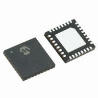
MRF89XA-I/MQ Microchip Technology, MRF89XA-I/MQ Datasheet - Page 24

MRF89XA-I/MQ
Manufacturer Part Number
MRF89XA-I/MQ
Description
TXRX ISM SUB-GHZ ULP 32QFN
Manufacturer
Microchip Technology
Specifications of MRF89XA-I/MQ
Package / Case
32-WFQFN Exposed Pad
Frequency
863MHz ~ 870MHz, 902MHz ~ 928MHz, 950MHz ~ 960MHz
Data Rate - Maximum
200kbps
Modulation Or Protocol
FSK, OOK
Applications
ISM
Power - Output
12.5dBm
Sensitivity
-113dBm
Voltage - Supply
2.1 V ~ 3.6 V
Current - Receiving
3mA
Current - Transmitting
25mA
Data Interface
PCB, Surface Mount
Antenna Connector
PCB, Surface Mount
Operating Temperature
-40°C ~ 85°C
Number Of Receivers
1
Number Of Transmitters
1
Wireless Frequency
863 MHz to 870 MHz, 902 MHz to 928 MHz, 950 MHz to 960 MHz
Interface Type
SPI
Noise Figure
- 112 dBc
Output Power
- 8.5 dBm, + 12.5 dBm
Operating Supply Voltage
2.1 V to 3.6 V
Maximum Operating Temperature
+ 85 C
Mounting Style
SMD/SMT
Maximum Data Rate
256 Kbps
Maximum Supply Current
25 mA
Minimum Operating Temperature
- 40 C
Modulation
FSK
Lead Free Status / RoHS Status
Lead free / RoHS Compliant
Memory Size
-
Lead Free Status / Rohs Status
Lead free / RoHS Compliant
Available stocks
Company
Part Number
Manufacturer
Quantity
Price
Company:
Part Number:
MRF89XA-I/MQ
Manufacturer:
MICROCHIP
Quantity:
12 000
2.11.1
Write Register - To write a value into a Configuration
register, the timing diagram illustrated in Figure 2-12
should be followed by the host microcontroller. The
new value of the register is effective from the rising
edge of CSCON.
FIGURE 2-12:
DS70622B-page 24
MRF89XA
Note:
CSCON (In)
SCK (In)
SDI (In)
SDO (Out)
SPI CONFIG
When writing more than one register suc-
cessively, it is not compulsory to toggle
CSCON back high between two write
sequences. The bytes are alternatively
considered as address and value. In this
instance, all new values will become effec-
tive on rising edge of CSCON.
(input)
HZ
* when writing the new value at address A1, the current content of A1 can be read by the µC.
start
1
x
WRITE REGISTER SEQUENCE
rw
2
x
A(4)
3
x
A(3)
Address = A1
4
x
(In)/(Out) refers to MRF89XA side
A(2)
5
x
A(1)
6
x
Preliminary
A(0)
7
x
stop
8
x
D(7) D(6) D(5)
D(7)
9
D(6) D(5)
10
11
Current value at
New value at
address A1
address A1*
D(4) D(3)
D(4) D(3)
12
13
© 2010 Microchip Technology Inc.
D(2) D(1)
D(2) D(1)
14
15
D(0)
16
D(0)
(input)
HZ


