MRF89XA-I/MQ Microchip Technology, MRF89XA-I/MQ Datasheet - Page 7
MRF89XA-I/MQ
Manufacturer Part Number
MRF89XA-I/MQ
Description
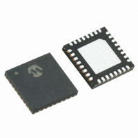
TXRX ISM SUB-GHZ ULP 32QFN
Manufacturer
Microchip Technology
Specifications of MRF89XA-I/MQ
Package / Case
32-WFQFN Exposed Pad
Frequency
863MHz ~ 870MHz, 902MHz ~ 928MHz, 950MHz ~ 960MHz
Data Rate - Maximum
200kbps
Modulation Or Protocol
FSK, OOK
Applications
ISM
Power - Output
12.5dBm
Sensitivity
-113dBm
Voltage - Supply
2.1 V ~ 3.6 V
Current - Receiving
3mA
Current - Transmitting
25mA
Data Interface
PCB, Surface Mount
Antenna Connector
PCB, Surface Mount
Operating Temperature
-40°C ~ 85°C
Number Of Receivers
1
Number Of Transmitters
1
Wireless Frequency
863 MHz to 870 MHz, 902 MHz to 928 MHz, 950 MHz to 960 MHz
Interface Type
SPI
Noise Figure
- 112 dBc
Output Power
- 8.5 dBm, + 12.5 dBm
Operating Supply Voltage
2.1 V to 3.6 V
Maximum Operating Temperature
+ 85 C
Mounting Style
SMD/SMT
Maximum Data Rate
256 Kbps
Maximum Supply Current
25 mA
Minimum Operating Temperature
- 40 C
Modulation
FSK
Lead Free Status / RoHS Status
Lead free / RoHS Compliant
Memory Size
-
Lead Free Status / Rohs Status
Lead free / RoHS Compliant
Available stocks
Company
Part Number
Manufacturer
Quantity
Price
Company:

Part Number:
MRF89XA-I/MQ
Manufacturer:
MICROCHIP
Quantity:
12 000


1.0
Microchip Technology's MRF89XA is a fully integrated,
half-duplex, sub-GHz transceiver. This low-power,
single chip FSK and OOK baseband transceiver
supports:
• Superheterodyne architecture
• Multi-channel, multi-band synthesizer with Phase
• Power Amplifier (PA)
• Low Noise Amplifier (LNA)
• I/Q two stage down converter mixers
• I/Q demodulator, FSK/OOK
• Baseband filters and amplifiers
The simplified block diagram of the MRF89XA is
illustrated in Figure 1-1.
The MRF89XA is a good choice for low-cost,
high-volume, low data rate (≤ 200 kbps), two-way short
range wireless applications. This device is a single chip
FSK and OOK transceiver capable of operation in the
863-870 MHz and 902-928 MHz license-free ISM
frequency bands, and the 950-960 MHz frequency
band.
The low-cost MRF89XA is optimized for very low-power
consumption (3 mA in Receive mode). It incorporates a
baseband modem with data rates up to 200 kbps in FSK
and 32 kbps in OOK. Data handling features include a
64-byte FIFO, packet handling, automatic CRC
generation and data whitening. The device also
supports Manchester coding techniques. Its highly
integrated architecture allows for minimum external
component count while still maintaining design flexibility.
All
programmable and most of them may be dynamically
set.
The MRF89XA supports a stable sensitivity and
linearity characteristics for a wide supply range and is
internally regulated. The frequency synthesizer of the
MRF89XA is a fully integrated integer-N type PLL. The
oscillator circuit provided on the MRF89XA device
provides the reference clock for the PLL. The
frequency synthesizer requires only five external
components which includes PLL loop filter and the
VCO tank circuit. Low phase noise provides for
excellent adjacent channel rejection capability, Bit Error
Rate (BER) and longer communication range.
© 2010 Microchip Technology Inc.
Lock Loop (PLL) for easy RF design
major
OVERVIEW
RF
communication
parameters
Preliminary
are
The high-resolution PLL allows:
• Usage of multiple channels in any of the bands
• Rapid settling time, which allows for faster
A communication link in most applications can be
created using a low-cost 12.8 MHz crystal, a SAW filter
and a low-cost microcontroller. The MRF89XA
provides a clock signal for the microcontroller. The
transceiver can be interfaced with many popular
Microchip PIC
Serial Peripheral Interface (SPI), interruptS (IRQ0 and
IRQ1), PLL lock and clock out. The interface between
the microcontroller and MRF89XA (a typical MRF89XA
RF node) is illustrated in Figure 1-2.
The MRF89XA supports the following digital data
processing features:
• Received Signal Strength Indicator (RSSI)
• Sync word recognition
• Packet handling
• Interrupt and flags
• Different operating Modes (Continuous, Buffer
• Data filtering/whitening/encoding
• Baseband power amplifier
• 64-byte TX/RX FIFO
The role of the digital processing unit is to interface the
data to/from the modulator/demodulator and the
microcontroller access points (SPI, IRQ and DATA pins).
It also controls all of the Configuration registers. The
receiver's Baseband Bandwidth (BBBW) can be
programmed to accommodate various deviations and
data rates requirements.
An optional Bit Synchronizer (BitSync) is provided, to
supply a synchronous clock and data stream to a
companion microcontroller in Continuous mode, or to
fill the FIFO with glitch-free data in Buffered mode. The
transceiver is integrated with different power-saving
modes and a software wake-up time through the host
microcontroller to keep track of the activities, which
reduces the overall current consumption and extends
the battery life. The small size and low-power
consumption of the MRF89XA makes it ideal for
various short range radio applications.
The MRF89XA complies with European (ETSI EN
300-220 V2.3.1) and United States (FCC Part 15.247
and 15.249) regulatory standards.
frequency hopping
and Packet)
®
microcontrollers through a 4-wire
MRF89XA
DS70622B-page 7
Related parts for MRF89XA-I/MQ
Image
Part Number
Description
Manufacturer
Datasheet
Request
R

Part Number:
Description:
Ultra-low Power, Integrated Ism Band Sub-ghz Transceiver
Manufacturer:
Microchip Technology Inc.
Datasheet:
Part Number:
Description:
Manufacturer:
Microchip Technology Inc.
Datasheet:
Part Number:
Description:
Manufacturer:
Microchip Technology Inc.
Datasheet:
Part Number:
Description:
Manufacturer:
Microchip Technology Inc.
Datasheet:
Part Number:
Description:
Manufacturer:
Microchip Technology Inc.
Datasheet:
Part Number:
Description:
Manufacturer:
Microchip Technology Inc.
Datasheet:
Part Number:
Description:
Manufacturer:
Microchip Technology Inc.
Datasheet:
Part Number:
Description:
Manufacturer:
Microchip Technology Inc.
Datasheet:
Part Number:
Description:
Manufacturer:
Microchip Technology Inc.
Datasheet: