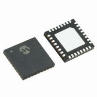
MRF89XA-I/MQ Microchip Technology, MRF89XA-I/MQ Datasheet - Page 95

MRF89XA-I/MQ
Manufacturer Part Number
MRF89XA-I/MQ
Description
TXRX ISM SUB-GHZ ULP 32QFN
Manufacturer
Microchip Technology
Specifications of MRF89XA-I/MQ
Package / Case
32-WFQFN Exposed Pad
Frequency
863MHz ~ 870MHz, 902MHz ~ 928MHz, 950MHz ~ 960MHz
Data Rate - Maximum
200kbps
Modulation Or Protocol
FSK, OOK
Applications
ISM
Power - Output
12.5dBm
Sensitivity
-113dBm
Voltage - Supply
2.1 V ~ 3.6 V
Current - Receiving
3mA
Current - Transmitting
25mA
Data Interface
PCB, Surface Mount
Antenna Connector
PCB, Surface Mount
Operating Temperature
-40°C ~ 85°C
Number Of Receivers
1
Number Of Transmitters
1
Wireless Frequency
863 MHz to 870 MHz, 902 MHz to 928 MHz, 950 MHz to 960 MHz
Interface Type
SPI
Noise Figure
- 112 dBc
Output Power
- 8.5 dBm, + 12.5 dBm
Operating Supply Voltage
2.1 V to 3.6 V
Maximum Operating Temperature
+ 85 C
Mounting Style
SMD/SMT
Maximum Data Rate
256 Kbps
Maximum Supply Current
25 mA
Minimum Operating Temperature
- 40 C
Modulation
FSK
Lead Free Status / RoHS Status
Lead free / RoHS Compliant
Memory Size
-
Lead Free Status / Rohs Status
Lead free / RoHS Compliant
Available stocks
Company
Part Number
Manufacturer
Quantity
Price
Company:
Part Number:
MRF89XA-I/MQ
Manufacturer:
MICROCHIP
Quantity:
12 000
3.13
Battery life can be greatly extended in MRF89XA appli-
cations where transmissions from field nodes are infre-
quent,
concentrated in periodic time slots. For example, field
nodes in many wireless alarm systems report opera-
tional status a few times a day, and can otherwise sleep
unless an alarm condition occurs. Sensor networks that
monitor parameters that change relatively slowly, such
as air and soil temperature in agricultural settings,
switching lights ON/OFF, only need to
updates a few times per an hour.
At room temperature, the MRF89XA draws a maximum
of 1 μA in Sleep mode, with a typical value of 100 nA.
To achieve minimum Sleep mode current, the CSCON
pin (pin 14), SDI pin (pin 17) and SCK pin (pin 18) must
be held logic low, while the CSDAT pin (pin 15) and
SDO pin (pin 16) must be held logic high.
The MRF89XA can go from Sleep mode through
Stand-by mode and Synthesizer mode to Transmit (or
Receive) mode in less than 6 ms. For configuring and
driving the device different operating modes refer to
Table 2-3. At a data rate of 33.33 kbps, a 32-byte
packet with a 4-byte preamble and a 4-byte start pat-
tern takes about 10 ms to transmit. Assume that the
MRF89XA then switches to Receive mode for one sec-
ond to listen for a response and returns to Sleep mode.
On the basis of reporting every six hours, the ON to
Sleep duty cycle is about 1:21,259, greatly extending
battery life over continuous transmit-receive or even
stand-by operation.
The required timing accuracy for the microcontrollers in
a sleep-cycled application depends on several factors:
• The required “time-stamp” accuracy of data
• If the base station and any routing nodes present
• If the base station and any routing nodes present
© 2010 Microchip Technology Inc.
reported by sleeping field nodes. R-C Sleep mode
timers built into many microcontrollers have a tol-
erance of ±20% or more. For applications that
require more accurate time-stamping, many
microcontrollers can run on a watch crystal during
Sleep mode and achieve time-stamp accuracies
better than one second per 24 hours.
in a network must sleep cycle in addition to the
field nodes. Watch crystal control will usually be
needed to keep all nodes accurately synchronized
to the active time slots.
in a network can operate continuously (AC pow-
ered, solar charged batteries), and a loose time
stamp accuracy is OK, the microcontrollers in
sleeping field nodes can usually operate from
internal low-accuracy R-C timers
Battery Power Management
Configuration Values
or
network
communications
can
transmit
Preliminary
be
.
Therefore, as previously mentioned, Sleep mode is the
lowest power consumption mode in which the clock
and all functional blocks of the device are disabled. In
case of an interrupt, the device wakes up, switches to
Active mode and an interrupt signal generated on the
IRQ pin indicates the change in state to the host micro-
controller. The source of the interrupt can be
determined by reading the status word of the device.
To reduce current consumption, the MRF89XA
should be placed in the low-power consuming Sleep
mode. In Sleep mode, the 12.8 MHz main oscillator
is turned OFF, disabling the RF and baseband cir-
cuitry. Data is retained in the control and FIFO regis-
ters and the transceiver is accessible through the
SPI port. The MRF89XA will not enter Sleep mode if
any interrupt remains active, regardless of the state
of the CLKOCNTRL bit (CLKOUTREG<7>). This
way, the microcontroller can always have a clock sig-
nal to process the interrupt. To prevent high-current
consumption, which results in shorter battery life, it is
highly recommended to process and clear interrupts
before entering Sleep mode. The functions which are
not necessary should be turned off to avoid
unwanted interrupts. To minimize current consump-
tion, the MRF89XA supports different power-saving
modes, along with an integrated wake-up timer.
When switching from Sleep mode to Stand-by, the crys-
tal oscillator will be active for no more than 5 ms.
Switching from Stand-by to Synthesizer mode, the PLL
will lock in less than 0.5 ms. PLL lock can be monitored
on the PLOCK pin (pin 23) of the MRF89XA. The radio
can then be switched to either Transmit or Receive
mode. When switching from any other mode back to
Sleep mode, the device will drop to its Sleep mode
current in less than 1 ms.
Note:
Many host microcontrollers cannot be
operated from the MRF89XA buffered
clock output if sleep cycling is planned. In
Sleep mode, the MRF89XA buffered clock
output is disabled, which will disable the
microcontroller unless it is capable of
automatically switching to an internal clock
source when external clocking is lost.
MRF89XA
DS70622B-page 95


