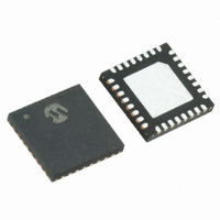
MRF89XA-I/MQ Microchip Technology, MRF89XA-I/MQ Datasheet - Page 19

MRF89XA-I/MQ
Manufacturer Part Number
MRF89XA-I/MQ
Description
TXRX ISM SUB-GHZ ULP 32QFN
Manufacturer
Microchip Technology
Specifications of MRF89XA-I/MQ
Package / Case
32-WFQFN Exposed Pad
Frequency
863MHz ~ 870MHz, 902MHz ~ 928MHz, 950MHz ~ 960MHz
Data Rate - Maximum
200kbps
Modulation Or Protocol
FSK, OOK
Applications
ISM
Power - Output
12.5dBm
Sensitivity
-113dBm
Voltage - Supply
2.1 V ~ 3.6 V
Current - Receiving
3mA
Current - Transmitting
25mA
Data Interface
PCB, Surface Mount
Antenna Connector
PCB, Surface Mount
Operating Temperature
-40°C ~ 85°C
Number Of Receivers
1
Number Of Transmitters
1
Wireless Frequency
863 MHz to 870 MHz, 902 MHz to 928 MHz, 950 MHz to 960 MHz
Interface Type
SPI
Noise Figure
- 112 dBc
Output Power
- 8.5 dBm, + 12.5 dBm
Operating Supply Voltage
2.1 V to 3.6 V
Maximum Operating Temperature
+ 85 C
Mounting Style
SMD/SMT
Maximum Data Rate
256 Kbps
Maximum Supply Current
25 mA
Minimum Operating Temperature
- 40 C
Modulation
FSK
Lead Free Status / RoHS Status
Lead free / RoHS Compliant
Memory Size
-
Lead Free Status / Rohs Status
Lead free / RoHS Compliant
Available stocks
Company
Part Number
Manufacturer
Quantity
Price
Company:
Part Number:
MRF89XA-I/MQ
Manufacturer:
MICROCHIP
Quantity:
12 000
2.7
The Interrupt Requests (IRQ0 and IRQ1) pins 21 and
22, respectively provide an interrupt signal to the host
microcontroller from the MRF89XA. Interrupt requests
are generated for the host microcontroller by pulling the
IRQ0 (pin 21) or IRQ1 (pin 22) pins low or high based
on the events and configuration settings of these
interrupts. Interrupts must be enabled and unmasked
before the IRQ pins are active. For detailed functional
description of interrupts see Section 3.8 “Data
Processing” .
2.8
After OOK or FSK demodulation, the baseband signal
is available to the user on the DATA pin (pin 20), when
Continuous mode is selected. Therefore, in Continuous
mode, the NRZ data to or from the modulator or
demodulator respectively is directly accessed by the
host microcontroller on the bidirectional DATA pin. The
SPI Data, FIFO and packet handler are therefore
inactive. In Buffered and Packet modes, the data is
retrieved from the FIFO through the SPI.
During transmission, the DATA pin is configured as
DATA (Data Out) and with internal Transmit mode
disabled; this manually modulates the data from the
external host microcontroller. If the Transmit mode is
enabled, this pin can be tied “high” or can be left
unconnected.
During reception, the DATA pin is configured as DATA
(Data In); this pin receives the data in conjunction with
DCLK. DATA pin (unused in packed mode) should be
pulled-up to VDD through a 100 kohm resistor.
FIGURE 2-6:
© 2010 Microchip Technology Inc.
RFIO
Interrupt (IRQ0 and IRQ1) Pins
DATA Pin
PA
Amplification
TRANSMITTER ARCHITECTURE BLOCK DIAGRAM
RF
up-conversion
Second
Q
I
LO1 TX
IF
up-conversion
Preliminary
First
Q
Q
I
I
2.9
The transmitter chain is based on the same
double-conversion architecture and uses the same
intermediate frequencies as the receiver chain. The
main blocks include:
A digital waveform generator that provides the I and Q
base-band
digital-to-analog converters and anti-aliasing low-pass
filters.
A compound image-rejection mixer to up-convert the
baseband signal to the first IF at one-ninth of the carrier
frequency (F
up-convert the IF signal to the RF frequency transmitter
driver and power amplifier stages to drive the antenna
port.
LO2 TX
LO2 TX
Interpolation
Transmitter
filters
rf
), and a second image-rejection mixer to
signals.
Baseband
DACs
This
MRF89XA
Waveform
Generator
DDS
block
DS70622B-page 19
includes
Data
Clock


