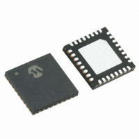
MRF89XA-I/MQ Microchip Technology, MRF89XA-I/MQ Datasheet - Page 76

MRF89XA-I/MQ
Manufacturer Part Number
MRF89XA-I/MQ
Description
TXRX ISM SUB-GHZ ULP 32QFN
Manufacturer
Microchip Technology
Specifications of MRF89XA-I/MQ
Package / Case
32-WFQFN Exposed Pad
Frequency
863MHz ~ 870MHz, 902MHz ~ 928MHz, 950MHz ~ 960MHz
Data Rate - Maximum
200kbps
Modulation Or Protocol
FSK, OOK
Applications
ISM
Power - Output
12.5dBm
Sensitivity
-113dBm
Voltage - Supply
2.1 V ~ 3.6 V
Current - Receiving
3mA
Current - Transmitting
25mA
Data Interface
PCB, Surface Mount
Antenna Connector
PCB, Surface Mount
Operating Temperature
-40°C ~ 85°C
Number Of Receivers
1
Number Of Transmitters
1
Wireless Frequency
863 MHz to 870 MHz, 902 MHz to 928 MHz, 950 MHz to 960 MHz
Interface Type
SPI
Noise Figure
- 112 dBc
Output Power
- 8.5 dBm, + 12.5 dBm
Operating Supply Voltage
2.1 V to 3.6 V
Maximum Operating Temperature
+ 85 C
Mounting Style
SMD/SMT
Maximum Data Rate
256 Kbps
Maximum Supply Current
25 mA
Minimum Operating Temperature
- 40 C
Modulation
FSK
Lead Free Status / RoHS Status
Lead free / RoHS Compliant
Memory Size
-
Lead Free Status / Rohs Status
Lead free / RoHS Compliant
Available stocks
Company
Part Number
Manufacturer
Quantity
Price
Company:
Part Number:
MRF89XA-I/MQ
Manufacturer:
MICROCHIP
Quantity:
12 000
3.7
Sync word recognition (also called pattern recognition)
is activated by setting the SYNCREN bit (SYN-
CREG<5>). The bit synchronizer must be activated.
The block behaves like a shift register; it continuously
compares the incoming data with its internally pro-
grammed Sync word and asserts the Sync IRQ source
on each occasion that a match is detected. This is illus-
trated in Figure 3-15.
During the comparison of the demodulated data, the
first bit received is compared with bit 7 (MSb) of the
byte at address 22 and the last bit received is com-
pared with bit 0 (LSb) of the last byte whose address is
determined by the length of the Sync word. When the
programmed Sync word is detected the user can
assume that this incoming packet is for the node and
can be processed accordingly.
3.7.1
Size: Sync word size can be set to 8, 16, 24 or 32 bits
through the SYNCWSZ<1:0> bits (SYNCREG<5:4>).
In Packet mode this field is also used for Sync word
generation in TX mode.
Error Tolerance: The number of errors tolerated in the
Sync word recognition can be set to 0, 1, 2 or 3 through
the SYNCTEN<1:0> bits (SYNCREG<2:1>).
Value: The Sync word value is configured in the Sync
Word Parameters in the related Configuration Regis-
ters. In Packet mode this field is also used for Sync
word generation in TX mode.
FIGURE 3-15:
DS70622B-page 76
MRF89XA
DCLK
RX DATA
(NRZ)
SYNC
Sync Word Recognition
CONFIGURATION
SSYNCVAL<x>
Bit N-x =
SYNC WORD RECOGNITION
SYNCVAL<0>
Bit N-1 =
Preliminary
SYNCVAL<0>
Bit N =
3.7.2
The packet handler is the block used in Packet mode.
Its functionality is described in Section 3.11 “Packet
Mode ”.
3.7.3
The control block configures and controls the behavior
of the MRF89XA according to the settings programmed
in the configuration registers.
3.7.4
The registers associated with SYNC are:
• GCONREG (Register 2-1)
• DMODREG (Register 2-2)
• FDEVREG (Register 2-3)
• BRSREG (Register 2-4)
• FLTHREG (Register 2-5)
• FIFOCREG (Register 2-6)
• FTXRXIREG (Register 2-14)
• FTPRIREG (Register 2-15)
• RSTHIREG (Register 2-16)
• FILCREG (Register 2-17)
• PFCREG (Register 2-18)
• SYNCREG (Register 2-19)
• RSTSREG (Register 2-21)
• OOKCREG (Register 2-22)
• SYNCV31REG (Register 2-23)
• SYNCV23REG (Register 2-24)
PACKET HANDLER
CONTROL
SYNC REGISTERS
© 2010 Microchip Technology Inc.


