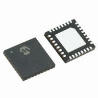
MRF89XA-I/MQ Microchip Technology, MRF89XA-I/MQ Datasheet - Page 94

MRF89XA-I/MQ
Manufacturer Part Number
MRF89XA-I/MQ
Description
TXRX ISM SUB-GHZ ULP 32QFN
Manufacturer
Microchip Technology
Specifications of MRF89XA-I/MQ
Package / Case
32-WFQFN Exposed Pad
Frequency
863MHz ~ 870MHz, 902MHz ~ 928MHz, 950MHz ~ 960MHz
Data Rate - Maximum
200kbps
Modulation Or Protocol
FSK, OOK
Applications
ISM
Power - Output
12.5dBm
Sensitivity
-113dBm
Voltage - Supply
2.1 V ~ 3.6 V
Current - Receiving
3mA
Current - Transmitting
25mA
Data Interface
PCB, Surface Mount
Antenna Connector
PCB, Surface Mount
Operating Temperature
-40°C ~ 85°C
Number Of Receivers
1
Number Of Transmitters
1
Wireless Frequency
863 MHz to 870 MHz, 902 MHz to 928 MHz, 950 MHz to 960 MHz
Interface Type
SPI
Noise Figure
- 112 dBc
Output Power
- 8.5 dBm, + 12.5 dBm
Operating Supply Voltage
2.1 V to 3.6 V
Maximum Operating Temperature
+ 85 C
Mounting Style
SMD/SMT
Maximum Data Rate
256 Kbps
Maximum Supply Current
25 mA
Minimum Operating Temperature
- 40 C
Modulation
FSK
Lead Free Status / RoHS Status
Lead free / RoHS Compliant
Memory Size
-
Lead Free Status / Rohs Status
Lead free / RoHS Compliant
Available stocks
Company
Part Number
Manufacturer
Quantity
Price
Company:
Part Number:
MRF89XA-I/MQ
Manufacturer:
MICROCHIP
Quantity:
12 000
3.12
Certain control register values must be initialized for
basic operations of the MRF89XA. These values differ
from the POR values and provide improved operational
parameters. These settings are normally made once
after a Reset. After initialization, the other features of
the MRF89XA device can be configured based on the
application. Accessing a register is implied as a com-
mand to the MRF89XA device through the SPI port.
The steps to initialize the MRF89XA using the control
registers are as follows:
1.
2.
3.
4.
5.
6.
7.
8.
9.
10. In the FILCREG register, enable the Passive
11. Configure RX parameters:
DS70622B-page 94
MRF89XA
In the GCONREG register:
a)
b)
c)
In the DMODREG register:
a)
b)
c)
d)
In the BRSREG register, program the Bit Rate
using the BRVAL<6:0> bits.
In the FLTHREG register, set the Floor Thresh-
old for OOK using the FTOVAL<7:0> bits.
In the FIFOCREG register, configure the FIFO
Size and FIFO Threshold using the FSIZE<1:0>
and FTINT<5:0> bits.
In the PACREG register, configure the Power
Amplifier Ramp Control using the PARC<1:0>
bits.
In the FTXRXIREG register:
a)
b)
In the FTPRIREG register:
a)
b)
In the RSTHIREG, program the RSSI Threshold
value
RTIVAL<7:0> bits.
Filter using the PASFILV<3:0> bits.
Initialization
Set the Chip Mode (CMOD<2:0>), Fre-
quency Band (FBS<1:0>) and VCO Trim
(VCOT<1:0>) bits.
Program the Frequency band.
Set the Trim bits to appropriately tune in the
VCO.
Select the Modulation Type using the MOD-
SEL<1:0> bits.
Enable DATA mode for Transmission using
the DMODE0 and DMODE1 bits.
Select gain for IF chain using the
IFGAIN<1:0> bits.
In the FDEVREG register, program the Fre-
quency Deviation bits (FDVAL<7:0>).
Configure the RX interrupts for IRQ0 and
IRQ1
IRQ1RXS<1:0> bits.
Configure the TX interrupts for IRQ1 using
the IRQ1TX bit.
Configure the TX interrupts for IRQ0 using
the IRQ0TXST bit.
Enable PLL Lock for interrupt on IRQ1
using the LENPLL bit.
for
using
interrupt
the
request
IRQ0RXS<1:0>
using
and
the
Preliminary
12. In
13. Configure TX parameters:
14. In the CLKOUTREG register, configure the
15. Configure the Packet Frame parameters in the
16. In the FCRCREG register, enable FIFO write
Note 1: Program registers 0x00 - 0x1F with
a)
b)
c)
d)
SYNCWSZ<1:0> = 11 for 32-bit SYNC word.
a)
b)
Clock Settings using the CLKOCNTRL and
CLKOFREQ<4:0> bits.
PLOADREG, NADDSREG, PKTCREG and
FCRCREG registers:
a)
b)
c)
d)
e)
f)
access using the FRWAXS bit.
2: Clear the PLL Lock flag by setting the
3: Program CMOD bits (GCONREG 0x00
4: Verify the PLL lock flag through the LST-
5: Program the CMOD bits (GCONREG
Enable Passive Filter with value as set in
step 11.
Set f
Enable SYNC and Set SYNC Word, Size,
Length and Tolerance.
Set configuration bytes for OOK Threshold
from OOKCREG
Change or Reset f
In the TXCONREG register, enable TX and
its
TXIPOLFV<3:0> and TXOPVAL<2:0> bits.
Enable Manchester Encoding
Set packet format and length of the packet
Set Node local address
Program preamble variables
Configure CRC parameters
Enable Address Filtering
the
appropriate settings. (General Configura-
tion
Packet Parameters).
LSTSPLL bit (FTPRIREG 0x0E<1>) to
‘1’.
<7:5>) to ‘0b010 Frequency Synthesizer
mode.
SPLL bit (FTPRIREG 0x0E<1>). If LST-
SPLL = 1, it implies that the MRF89XA is
ready to operate at the frequency indi-
cated by the Ri/Pi/Si register set.
0x00 <7:5>) to ‘0b001 Standby mode.
c
and f
transmit
Parameters,
SYNCREG
o
.
© 2010 Microchip Technology Inc.
c
.
power
IRQ
register,
using
Parameters,
the
set


