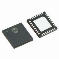
MRF89XA-I/MQ Microchip Technology, MRF89XA-I/MQ Datasheet - Page 62

MRF89XA-I/MQ
Manufacturer Part Number
MRF89XA-I/MQ
Description
TXRX ISM SUB-GHZ ULP 32QFN
Manufacturer
Microchip Technology
Specifications of MRF89XA-I/MQ
Package / Case
32-WFQFN Exposed Pad
Frequency
863MHz ~ 870MHz, 902MHz ~ 928MHz, 950MHz ~ 960MHz
Data Rate - Maximum
200kbps
Modulation Or Protocol
FSK, OOK
Applications
ISM
Power - Output
12.5dBm
Sensitivity
-113dBm
Voltage - Supply
2.1 V ~ 3.6 V
Current - Receiving
3mA
Current - Transmitting
25mA
Data Interface
PCB, Surface Mount
Antenna Connector
PCB, Surface Mount
Operating Temperature
-40°C ~ 85°C
Number Of Receivers
1
Number Of Transmitters
1
Wireless Frequency
863 MHz to 870 MHz, 902 MHz to 928 MHz, 950 MHz to 960 MHz
Interface Type
SPI
Noise Figure
- 112 dBc
Output Power
- 8.5 dBm, + 12.5 dBm
Operating Supply Voltage
2.1 V to 3.6 V
Maximum Operating Temperature
+ 85 C
Mounting Style
SMD/SMT
Maximum Data Rate
256 Kbps
Maximum Supply Current
25 mA
Minimum Operating Temperature
- 40 C
Modulation
FSK
Lead Free Status / RoHS Status
Lead free / RoHS Compliant
Memory Size
-
Lead Free Status / Rohs Status
Lead free / RoHS Compliant
Available stocks
Company
Part Number
Manufacturer
Quantity
Price
Company:
Part Number:
MRF89XA-I/MQ
Manufacturer:
MICROCHIP
Quantity:
12 000
TABLE 3-1:
3.2.6.1
To ensure that the frequency band of operation may be
accurately addressed by the R, P, and S dividers of the
synthesizer, it is necessary to ensure that the VCO is
correctly centered. The MRF89XA built-in VCO
trimming feature makes it easy and is controlled by the
SPI interface. This tuning does not require any RF test
equipment, and can be achieved by measuring Vtune,
the voltage between the PLLN and PLLP pins (6 and 7
pins).
The VCO is centered if the voltage is within the range
of 50 ≤ Vtune(mV) ≤ 150.
This measurement should be conducted when in
transmit mode at the center frequency of the desired
band (for example, approximately 867 MHz in the
863-870 MHz band), with the appropriate frequency
band
(GCONREG<4:3>).
If this inequality is not satisfied, adjust the VCOT<1:0>
bits (GCONREG<2:0>) from ‘00’ by monitoring Vtune.
This allows the VCO voltage to be trimmed in +60 mV
increments.
inaccessible, the voltage may be adjusted further by
changing the tank circuit inductance value.
An increase in inductance results in an increase Vtune.
In addition, for mass production, the VCO capacitance
is piece-to-piece dependant. As such, the optimization
proposed above should be verified on several
prototypes, to ensure that the population is centered
with 100 mV.
The register associated with VCO is:
• GCONREG (Register 2-1).
3.2.7
As illustrated in Figure 2-5, the PLL structure com-
prises three different dividers, R, P, and S, which set
the output frequency through the LO. A second set of
dividers is also available to allow rapid switching
between a pair of frequencies: R1/P1/S1 and
R2/P2/S2. These six dividers are programmed by six
independent registers (see Register 2-7 through
Register 2-12), which are selected by GCONREG.
DS70622B-page 62
MRF89XA
Target Channel
863-870
902-915
915-928
950-960
(MHz)
setting
FREQUENCY CALCULATION
Trimming
Hardware and Software
If
FREQUENCY BAND SETTING
the
using
desired
FBS1
1
0
0
1
the
the
VCO
voltage
(FBS<1:0>
FBS0
Tank
range
0
0
1
0
Preliminary
bits
by
is
FSK Mode
The formula provided in Equation 3-1 gives the
relationship between the local oscillator, and R, P and
S values, when using FSK modulation.
EQUATION 3-1:
3.2.8
The registers associated with FSK mode are:
• GCONREG (Register 2-1)
• DMODREG (Register 2-2).
OOK Mode
Due to the manner in which the baseband OOK
symbols are generated, the signal is always offset by
the FSK frequency deviation (FDVAL<7:0> as
programmed in FDEVREG<7:0>). Therefore, the
center of the transmitted OOK signal is represented by
Equation 3-2.
EQUATION 3-2:
Consequently, in Receive mode, due to the low
intermediate frequency (Low-IF) architecture of the
MRF89XA, the frequency should be configured so as to
ensure the correct low-IF receiver baseband center
frequency, IF2, as shown in Equation 3-3.
EQUATION 3-3:
As described in Section 3.4.4 “Channel Filters”, it is
recommended that IF2 be set to 100 kHz.
3.2.9
The registers associated with OOK mode are:
• GCONREG (Register 2-1)
• DMODREG (Register 2-2)
• FLTHREG (Register 2-5)
• OOKCREG (Register 2-22)
f
rf ook rx
f
,
rf ook tx
,
,
f
rf fsk
FSK MODE REGISTERS
,
OOK MODE REGISTERS
,
f
rf ook rx
=
,
f
=
rf ook tx
9
-- -
8
=
,
f
9
-- -
8
×
rf fsk
,
9
-- -
8
,
×
------------ -
R
f
×
,
xtaL
------------ -
R
f
+
xtaL
------------ -
R
=
f
© 2010 Microchip Technology Inc.
+
xtaL
1
=
+
=
9
-- -
8
[
1
75 ∗ P
9
-- - f
8
1
[
×
9
-- -
8
75 ∗ P
[
lo
75 ∗ P
×
f
(
lo
f
(
–
lo
(
IF2
+
–
+
1
f
+
dev
)
1
+
1
)
)
+
S
+
] IF2
S
–
S
] f
]
–
dev


