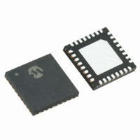
MRF89XA-I/MQ Microchip Technology, MRF89XA-I/MQ Datasheet - Page 21

MRF89XA-I/MQ
Manufacturer Part Number
MRF89XA-I/MQ
Description
TXRX ISM SUB-GHZ ULP 32QFN
Manufacturer
Microchip Technology
Specifications of MRF89XA-I/MQ
Package / Case
32-WFQFN Exposed Pad
Frequency
863MHz ~ 870MHz, 902MHz ~ 928MHz, 950MHz ~ 960MHz
Data Rate - Maximum
200kbps
Modulation Or Protocol
FSK, OOK
Applications
ISM
Power - Output
12.5dBm
Sensitivity
-113dBm
Voltage - Supply
2.1 V ~ 3.6 V
Current - Receiving
3mA
Current - Transmitting
25mA
Data Interface
PCB, Surface Mount
Antenna Connector
PCB, Surface Mount
Operating Temperature
-40°C ~ 85°C
Number Of Receivers
1
Number Of Transmitters
1
Wireless Frequency
863 MHz to 870 MHz, 902 MHz to 928 MHz, 950 MHz to 960 MHz
Interface Type
SPI
Noise Figure
- 112 dBc
Output Power
- 8.5 dBm, + 12.5 dBm
Operating Supply Voltage
2.1 V to 3.6 V
Maximum Operating Temperature
+ 85 C
Mounting Style
SMD/SMT
Maximum Data Rate
256 Kbps
Maximum Supply Current
25 mA
Minimum Operating Temperature
- 40 C
Modulation
FSK
Lead Free Status / RoHS Status
Lead free / RoHS Compliant
Memory Size
-
Lead Free Status / Rohs Status
Lead free / RoHS Compliant
Available stocks
Company
Part Number
Manufacturer
Quantity
Price
Company:
Part Number:
MRF89XA-I/MQ
Manufacturer:
MICROCHIP
Quantity:
12 000
2.10
The receiver is based on a superheterodyne architec-
ture and comprises the following major blocks:
• An LNA that provides low-noise RF gain followed
• A first mixer, which down-converts the RF signal
• A variable gain first-IF preamplifier followed by
• A two-stage IF filter followed by an amplifier chain
• An FSK arctangent type demodulator driven from
FIGURE 2-8:
© 2010 Microchip Technology Inc.
by an RF band-pass filter.
to an intermediate frequency equal to one-ninth of
the carrier frequency (F
signals).
two second mixers, which down-convert the first
IF signal to I and Q signals at a low frequency
(zero-IF for FSK, low-IF for OOK).
are available for both I and Q channels. Limiters
at the end of each chain drive the I and Q inputs
to the FSK demodulator function. An RSSI signal
is also derived from the I and Q IF amplifiers to
drive the OOK detector. The second filter stage in
each channel can be configured as either a
third-order Butterworth low-pass filter for FSK
operation
band-pass filter for OOK operation.
the I and Q limiter outputs, and an OOK demodu-
lator driven by the RSSI signal. Either detector
can drive a data and clock recovery function that
provides matched filter enhancement of the
demodulated data.
LNA
RF
Receiver
down-conversion
LO1 RX
or
First
an
RECEIVER ARCHITECTURE BLOCK DIAGRAM
image
IF1
rf
down-conversion
100 MHz for 915 MHz
Second
reject
LO2 RX
polyphase
Preliminary
RSSI
2.10.1
Figure 2-8 illustrates the receiver architecture block
diagram. The first IF is one-ninth of the RF frequency
(approximately
down-conversion down-converts the I and Q signals to
baseband in the case of the FSK receiver (zero-IF) and
to a low-IF (IF2) for the OOK receiver.
After the second down-conversion stage, the received
signal is channel-select filtered and amplified to a level
adequate for demodulation. Both FSK and OOK
demodulation are available. Finally, an optional bit
synchronizer (BitSync) is provided, to supply a
synchronous clock and data stream to a companion
microcontroller in Continuous mode, or to fill the FIFO
buffers with glitch-free data in Buffered mode.
Baseband, IF2 in OOK
Note:
Demod
Demod
OOK
FSK
RECEIVER ARCHITECTURE
Image rejection is achieved by using a
SAW filter on the RF input.
100 MHz).
BitSync
MRF89XA
Control Logic
- FIFO Handler
- SPI Interface
- Packet Handler
- Pattern Recognition
DS70622B-page 21
The
second


